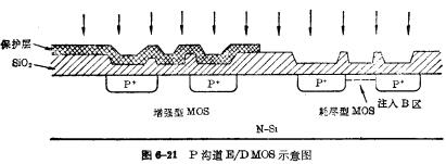
Ion implantation method to manufacture E/DMOS circuit analysis, it is much more difficult to manufacture enhanced and depleted MOS devices with the same channel on the same substrate, that is, E/D typ
Ion implantation method to manufacture E/DMOS circuit analysis, it is much more difficult to manufacture enhanced and depleted MOS devices with the same channel on the same substrate, that is, E/D typ
SOS technology manufacturing CMOS circuit process analysis, SOS technology is the abbreviation of "Epitaxial Silicon on Sapphire". This technique is to epitaxially grow a thin layer of silicon single
SOS technology manufacturing CMOS circuit process analysis, SOS technology is the abbreviation of "Epitaxial Silicon on Sapphire". This technique is to epitaxially grow a thin layer of silicon single
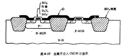
Ion implantation method for manufacturing CMOS circuit analysis, in the conventional process, the P-well region is formed by light boron diffusion, and the error of the diffusion concentration is rela
Ion implantation method for manufacturing CMOS circuit analysis, in the conventional process, the P-well region is formed by light boron diffusion, and the error of the diffusion concentration is rela
CMOS process, CMOS process flow, CMOS circuit is a combination of P-channel devices and N-channel devices. It has outstanding advantages such as high speed, low power consumption, and strong anti-inte
CMOS process, CMOS process flow, CMOS circuit is a combination of P-channel devices and N-channel devices. It has outstanding advantages such as high speed, low power consumption, and strong anti-inte
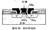
AMOS process, AMOS process flow, 1. The main features of AI2O3 AMOS process is a process that uses a SiO2-AI2O3 double-layer structure as the gate dielectric for MOS devices. The use of this process i
AMOS process, AMOS process flow, 1. The main features of AI2O3 AMOS process is a process that uses a SiO2-AI2O3 double-layer structure as the gate dielectric for MOS devices. The use of this process i
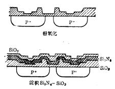
NMOS process, NMOS process devices, NMOS process is a process that uses SiO2-Si3N4 double-layer structure as the gate dielectric of MOS devices. This process is mainly based on the fact that silicon n
NMOS process, NMOS process devices, NMOS process is a process that uses SiO2-Si3N4 double-layer structure as the gate dielectric of MOS devices. This process is mainly based on the fact that silicon n
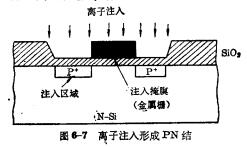
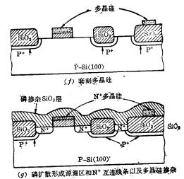
The MOS source and drain regions realize gate self-alignment and self-alignment mosfet. The source and drain regions of the MOS device are fabricated by ion implantation, and the gate self-alignment c
The MOS source and drain regions realize gate self-alignment and self-alignment mosfet. The source and drain regions of the MOS device are fabricated by ion implantation, and the gate self-alignment c
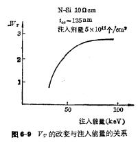
The application of VT of MOS devices, in the MOS process, ion implantation technology can not only be used to make NMOS or PMOS source and drain regions and CMOS P-well regions, but also can control a
The application of VT of MOS devices, in the MOS process, ion implantation technology can not only be used to make NMOS or PMOS source and drain regions and CMOS P-well regions, but also can control a
N-channel MOS, silicon gate N-channel MOS technology, N-channel and other planar processes, also known as "selective oxidation MOS technology", its characteristic is that a certain part of the silicon
N-channel MOS, silicon gate N-channel MOS technology, N-channel and other planar processes, also known as "selective oxidation MOS technology", its characteristic is that a certain part of the silicon
The P-channel "silicon gate process" has more characteristics for the performance of devices and integrated circuits than the conventional aluminum gate process. "Silicon gate process" has more charac
The P-channel "silicon gate process" has more characteristics for the performance of devices and integrated circuits than the conventional aluminum gate process. "Silicon gate process" has more charac


5C1, CD Block, Tianji Building, Tianan Digital City, Futian District, Shenzhen

KIA-The Public