Electronic Technology Forum
Analysis of process method for manufacturing E/DMOS circuit by ion implantation
It is more difficult to manufacture enhanced and depleted MOS devices with the same channel on the same substrate, that is, E/D-type MOS circuits. many. Therefore, in the early stage of the development of MOS technology, the development speed of E/DMOS circuits is relatively slow. However, with the rapid development of MOS technology, there are currently several process methods for manufacturing E/DMOS circuits.
1, P-channel E/DMOS
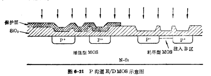
First, according to the conventional process of P-channel enhancement mode MOS, the gate is oxidized until the gate is oxidized, and then the depletion mode MOS load device is manufactured, that is, boron is carried out in the channel region of the load tube. Ion Implantation. The enhanced device is protected by photoresist, and other areas are protected by a thick oxide layer, and ions cannot pass through these areas. In this way, the channel region of the load tube is doped into P-type, forming a depletion-type MOS.
Because the V; value of aluminum-gate P-channel enhancement mode MOS devices is relatively large, the value of Vr must first be reduced by ion implantation. Therefore, after the gate oxidation (~120nm), the first boron implantation is performed to reduce the threshold voltage values of the two devices, and then phosphorous treatment is performed. Phosphosilicate glass is used as the mask of the enhanced device, and then the second step is performed. Secondary implantation to form a depletion MOS device. Process of E/DMOS circuit. After implantation, it is annealed in dry nitrogen at 950°C for 10 minutes. Fig. 6-21 is a schematic diagram of ion implantation to manufacture P-channel E/DMOS.

2, N-channel E/DMOS
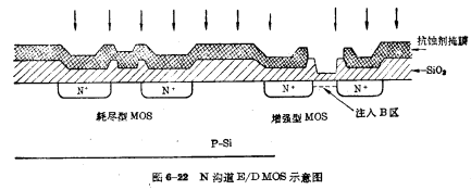
N-channel E/DMOS circuits can also be made with ion implantation technology. As we all know, N-channel MOS devices are easy to make depletion type, so P-type impurities can be injected where the original channel is not formed to increase the doping concentration of the channel region. As shown in Figure 6-22.

Contact: Mr. Zou
Tel: 0755-83888366-8022
Mobile: 18123972950
QQ: 2880195519
Address: 5C1, CD Block, Tianji Building, Tian’an Digital City, Chegongmiao, Futian District, Shenzhen
Please search the WeChat official account: "KIA Semiconductor" or scan the picture below to "Follow" the official WeChat official account
Please "Follow" the official WeChat account: provide MOS tube technical assistance


