Electronic Technology Forum
Threshold of MOS devices Voltage VT ion implantation adjustment method
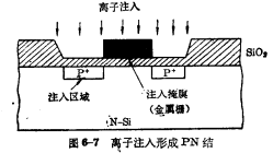
Ion implantation is the use of certain impurities (such as boron and phosphorus) atoms to cause electron impact ionization by gas discharge to generate charged impurity ions, and then under the action of a strong electric field, make The ions are accelerated to have a very high energy (about tens of thousands to hundreds of thousands of electron volts) and directly bombard the surface of the semiconductor material silicon. Application of VT for MOS devices. When these ions are implanted into the silicon body, they stay in the silicon surface layer because they are blocked by silicon atoms, play a doping role, and form a PN junction, as shown in Figure 6-7.

Ion implantation and doping, no lateral diffusion, thus eliminating the conventional The coverage caused by the drain area generates a capacitor, which is beneficial to improve the switching response of the MOS device. Ion implantation to form the PN junction implantation method also has the advantage of "gate self-alignment". The gate electrode of the device can be fabricated first, and then the source and drain regions can be fabricated, thereby overcoming the difficulty of mask alignment in the conventional process. Ion implantation can be performed at low temperatures, which can reduce thermal defects introduced by high-temperature diffusion. Also because the ion implantation method can form a PN junction under the passivation layer (such as thin silicon dioxide), the silicon surface is not easy to be contaminated, which ensures the stability of the device performance. In addition, the ion implantation technology has far more accurate control of the semiconductor doping concentration and junction depth than the general diffusion method, and the repeatability and uniformity are good, which can greatly improve the yield. Therefore, ion implantation technology has developed into one of the necessary process methods.
In the MOS process, ion implantation technology can not only be used to make NMOS or PMOS source and drain regions and CMOS P-well regions, but also can control a lower threshold voltage V T to facilitate compatibility with TTL circuits. As long as this technology makes minor changes to the conventional process, it can be easily matched with other MOS processes to produce enhanced and depleted devices (ie E/DMOS circuits) with the same type of channel on a single wafer. Application of VT for MOS devices. If the ion beam is focused very finely, narrow beam scanning is used for selective implantation, it becomes a maskless manufacturing technology, which greatly simplifies the production process of MOS large-scale integrated circuits. This section mainly introduces the application of ion implantation technology in MOS process.
One. Adjust the VT of MOS devices by ion implantation
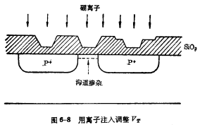
Threshold voltage of MOS devicesVT , and the amount of charge doped in the channel  Is proportional. Therefore, we can use ion implantation technology to enhance or compensate the doping concentration of the silicon substrate in the channel region of the MOS device, thereby effectively controlling and adjusting the threshold voltage of the MOS device. Application of VT for MOS devices. The specific method is to use a medium of appropriate thickness (such as metal layer, thick silicon dioxide or photoresist, etc.) as a masking film to prevent high-energy ion beams from penetrating those areas that do not need to be implanted, and ion beam implantation To the predetermined channel area. In this way, the doping concentration of the channel region can be adjusted, as shown in Figure 6-8.

Use ion implantation to adjust the device VT, usually before opening the photoetching lead hole. Dense ions are implanted into the channel region through the gate oxide thin layer, so that the N-type substrate in the channel is compensated. The other areas are thick oxide layers, and boron ions cannot be implanted into the silicon substrate in these areas. NextThe process of the surface is roughly the same as the conventional process.
How much ions need to be injected to achieve the expected lowerVT? Obviously, you can go directly from VT Derived from the expression.
Suppose a P-channel MOS device adopts aluminum gate, and the channel is impregnated. , surface potential
 , N-type substrate concentration
 , gate oxidethe thickness of the layer
 , the number of equivalent positive charges
 (equivalent to
  ), oxide layer capacitance
 . If threshold voltage is required
 , what is the positive charge density to be injected?
将上式数据代入VT表达式

可求得
 Yes Negative value. Indicates that the net charge must be negative when the channel region is depleted. In other words, when you want to VT=-2VWhen the corresponding The net space charge on the silicon surface of the channel region should be
  . This means that the channel region substrate has changed from N-type to weak P-type. Application of VT for MOS devices. Therefore, ion implantation is to first compensate the substrate in the channel region to become intrinsic silicon, and then further implant, and then make the substrate in the channel region become weak P-type. Due to the original N-type substrate
  , depletion zone charges can be generated
  , so the ionized charge density of injected boron is:

In this way, after offsetting the original charge in the depleted area of the substrate, the rest is exactly equivalent to 
 is slightly higher. Because not all ions injected into the crystal lattice can be electrically activated.
in In the case of implantation, will a residual channel appear and the device will become depleted? Will not. Because when there is no negative bias applied to the gate, due to the contact potential difference and the effective positive charge in the oxide layer
  is that the channel region is still N-type, ensuring that the device is still enhanced.
Because the ion implantation process to adjust the threshold voltage is performed after the gate oxidation, high-energy ions must be implanted into the substrate through a thin silicon dioxide layer. Application of VT for MOS devices. So the implant dose is related to the oxide layer thickness and implant energy. Figure 6-9 shows the relationship between the threshold voltage change and the injection energy for a certain oxide layer thickness (125nm), and Figure 6-10 shows the threshold voltage change and the silicon dioxide layer at a certain injection energy (44keV) The thickness of the relationship. After implantation, in order to eliminate the lattice damage and activate the ions, it is necessary to anneal at a temperature of 500 to 900°C for 10 to 20 minutes.
Contact: Mr. Zou
Tel: 0755-83888366-8022
Mobile: 18123972950
QQ: 2880195519
Address: 5C1, CD Block, Tianji Building, Tian’an Digital City, Chegongmiao, Futian District, Shenzhen
Please search the WeChat official account: "KIA Semiconductor" or scan the picture below to "Follow" the official WeChat official account
Please "Follow" the official WeChat account: provide MOS tube technical assistance


