Silicon gate process, the advantage of silicon gate process, "silicon gate process" is a process that uses doped polysilicon to make the gate electrode of the MOS tube. The difference from the convent
Silicon gate process, the advantage of silicon gate process, "silicon gate process" is a process that uses doped polysilicon to make the gate electrode of the MOS tube. The difference from the convent
NMOS process, the advantages and disadvantages of NMOS, N-channel process is an earlier choice process for MOS circuits, because theoretically the electron mobility is much higher, and it can be made
NMOS process, the advantages and disadvantages of NMOS, N-channel process is an earlier choice process for MOS circuits, because theoretically the electron mobility is much higher, and it can be made
PMOS technology, PMOS advantages and disadvantages, in the development process of MOS circuits, the earliest and fastest development is PMOS integrated circuits. The production of PMOS circuits is bas
PMOS technology, PMOS advantages and disadvantages, in the development process of MOS circuits, the earliest and fastest development is PMOS integrated circuits. The production of PMOS circuits is bas

A brief introduction to the basic principles of VLSI design, the speed of MOS technology development is amazing, and the performance and integration of MOS integrated circuits are about to double ever
A brief introduction to the basic principles of VLSI design, the speed of MOS technology development is amazing, and the performance and integration of MOS integrated circuits are about to double ever
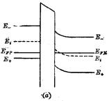
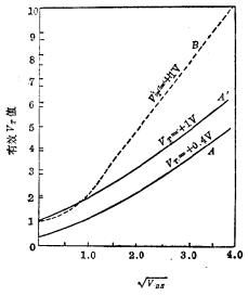
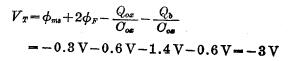
In the design of CMOS threshold voltage, in order to make the designed circuit layout meet the design index requirements in terms of performance, process design must be carried out to determine reason
In the design of CMOS threshold voltage, in order to make the designed circuit layout meet the design index requirements in terms of performance, process design must be carried out to determine reason
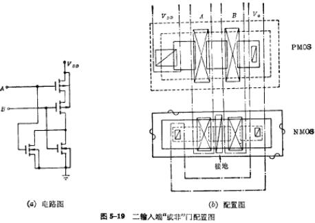
CMOS layout design, CMOS layout design overview, CMOS is a micro-power circuit, and the requirements for power consumption are particularly strict. The main factor causing high power consumption is st
CMOS layout design, CMOS layout design overview, CMOS is a micro-power circuit, and the requirements for power consumption are particularly strict. The main factor causing high power consumption is st
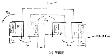
CMOS circuit devices, CMOS circuit calculation methods, design CMOS circuits, in general, according to user requirements and given circuit indicators, first design each device in the circuit, then dra
CMOS circuit devices, CMOS circuit calculation methods, design CMOS circuits, in general, according to user requirements and given circuit indicators, first design each device in the circuit, then dra
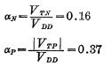
PMOS layout, PMOS layout design PMOS layout design device manufacturing method, layout design is in accordance with the design requirements and process conditions, select the appropriate size, determi
PMOS layout, PMOS layout design PMOS layout design device manufacturing method, layout design is in accordance with the design requirements and process conditions, select the appropriate size, determi

The design of PMOS integrated circuits, the layout of PMOS integrated circuits, and the design of MOS integrated circuits should generally include logic design, device design, layout design and proces
The design of PMOS integrated circuits, the layout of PMOS integrated circuits, and the design of MOS integrated circuits should generally include logic design, device design, layout design and proces
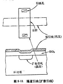
CCD application overview, charge-coupled device CCD, the application of CCD is mainly based on its three unique effects-storage effect, transfer effect and photoelectric effect, currently mainly used
CCD application overview, charge-coupled device CCD, the application of CCD is mainly based on its three unique effects-storage effect, transfer effect and photoelectric effect, currently mainly used


5C1, CD Block, Tianji Building, Tianan Digital City, Futian District, Shenzhen

KIA-The Public