Electronic Technology Forum
Analysis of CMOS circuit manufactured by ion implantation
In the conventional process, the P-well region is formed by light boron diffusion, the error of the diffusion concentration is relatively large, and it must be accurately controlled at 1015pcs/cm2The left and right are more difficult, making it difficult to match the threshold voltage. Therefore, it is necessary to use ion implantation to form P-wells to replace lightboron Diffusion. CMOS circuit. Because the dose of ion implantation can be controlled very accurately, the consistency of the threshold voltage of the N-channel MOS tube is greatly improved.
The dose of ion implantation can be based on the threshold voltage the requirements are calculated. For a silicon substrate with a (100) crystal plane,
 ,Require
 ,Calculate according to the threshold voltage formula:

Finally obtained:

Because of the substrate concentration , can provide depleted charge of
  . Ion implantation must first compensate for this part of the charge, and then further implant to make
  Reach
Reach  , so the total injection dose should be
  . CMOS circuit. If the scattering and related implanted ions are not activated, the actual implanted dose should be slightly larger than this value.
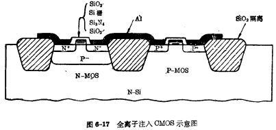
Figure 6-17 shows the use of ion implantation, isoplanar technology, silicon gate technology and SiO2-Si3N4 Structure diagram of an oxide-isolated CMOS circuit. It has good circuit performance, high integration and strong reliability, but the process steps are more complicated.

In the process, the formation of the P-well and the source and drain of the MOS device adopt ion implantation technology. The isolation between devices uses selective oxidation technology to make SiO2 buried in the silicon body, leaving the silicon mesa separated by field oxide isolation. Then ion implantation is used to form MOS devices on the silicon mesa. This gives play to the advantages of selective oxidation. The surface of the wafer is relatively flat, which overcomes the shortcomings of thick oxide step disconnection in common processes. CMOS circuit. The gate electrode adopts silicon gate technology and Si3N4 interlayer to form SiO2-multi-product silicon-Si3N4-SiO2 structure.
Only two CMOS processes are introduced above, and some other CMOS process method is basically a different combination of the above methods.
Contact: Mr. Zou
Tel: 0755-83888366-8022
Mobile: 18123972950
QQ: 2880195519
Address: 5C1, CD Block, Tianji Building, Tian’an Digital City, Chegongmiao, Futian District, Shenzhen
Please search the WeChat official account: "KIA Semiconductor" or scan the picture below to "Follow" the official WeChat official account
请“关注”官方微信公众号:提供 MOS管 技术帮助


