Electronic Technology Forum
CMOS process flow and process conditions analysis
CMOS circuit is a combination of P-channel devices and N-channel devices. It has outstanding advantages such as high speed, low power consumption, and strong anti-interference ability.
1. Basic CMOS process description
In the conventional CMOS process, the surface charge has a great influence on the threshold voltage value. Knowing from the previous discussion, the (111) side The typical value is 4×10¹¹/cm2, and the (100) surface
 It is 1×10¹¹ pieces/cm3.
If the resistivity p is 10Ω.cm N-type substrate (ie  ), the thickness of the gate oxide layer
 ,
, . For aluminum gate PMOS transistors,
  .
.
According to the Vr formula, it can be obtained:


For aluminum gate NMOS tubes, the surface concentration of the P-well region is 
 , It can be counted as:

It can be seen that it is much more difficult to make CMOS with (111) crystal face N-type silicon wafer than (100) crystal face. In order to facilitate the realization of P-channel and N-channel enhancement mode operation and threshold voltage matching. Therefore, Si material with (100) crystal plane is used as the substrate.
1, CMOS process flow
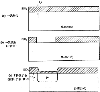
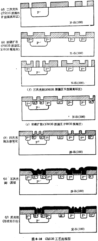
Picture6-16 represents the basic steps of the CMOS conventional process, the description is as follows:
①N-type silicon wafer with crystal orientation of<100>, resistivity p=10Ω·cm, after cutting, grinding and polishing, it is oxidized once to grow about 1μm Thick oxide layer;
②One photolithography, engrave the P-well area;
③The P-well area is diffused, and the surface concentration is controlled at  Range, knot depth is 10μm Left and right;
④Secondary photolithography, engrave the source and drain regions of P-channel MOS transistors and P-type isolation ring to prevent parasitic effects;
⑥The concentrated boron diffuses to form the source and drain regions of the PMOS tube and the isolation ring of the NMOS tube;
⑥Three times of photolithography, the source and drain regions of the N-channel MOS transistor and the N-type isolation ring are carved out;
⑦Concentrated phosphorus diffuses to form the source and drain regions of the NMOS tube and the isolation ring of the PMOS tube;
⑧Four times of photolithography, the gate area and pre-etched lead holes are carved out, followed by gate oxidation and phosphorous treatment to form a thin oxide layer with low charge density, the thickness of the gate oxide layer< img src="/userfiles/images/2020/12/02/2020120215302916.png" title="image.png" alt="image.png"/>About;
⑨Five times of photoetching, engraving lead holes, and steaming aluminum;
⑩Inversely engrave aluminum to form gate electrodes and interconnections. To ensure good ohmic contact, alloys are made.
Finally, it is packaged after dicing and ultrasonic bonding.


2, main process conditions
(1) Cleaning process
In the CMOS process, in order to obtain a low surface state density, (100) crystal orientation silicon wafers are used, but special attention must be paid to the cleaning process. Much stricter than PMOS circuits. Because the matching degree of the threshold voltage of the two MOS, the characteristics of the N-channel MOS, and the leakage situation are closely related to the cleaning of each process.
(2) Oxidation process
The first oxidation is used as a masking layer for P- trap light B diffusion. Because boron redistribution is at 1200℃, it takes about 8 hours, which is a long time. Therefore, the thickness of SiO2 is required to be 1μm.
The performance of the device has a lot to do with the quality of the gate oxide. The increase in the effective positive charge density in the gate oxide  will reduce the N-channel Channel MOS device
  , while making P-channel MOS device
  Ascend. Therefore, the control of
  is directly related to whether the threshold voltage of the two CMOS devices The problem of matching. Therefore, special attention must be paid to the cleaning of the gate oxide layer to ensure a low-density surface state. The thickness of the gate oxide layer is generally about 150 nm. The cleaning of silicon wafers before oxidation and the cleaning of the oxidation system must be strictly required. At the same time, there should be a phosphorus treatment process to improve the degree of sodium ion contamination of the oxide layer. It can also be described in
  Oxidize in an atmosphere.
(3) Diffusion process
①Light boron diffusion, that is, P-well diffusion
This is the most important step in the manufacture of CMOS circuits. The diffused junction is deeper, so the concentration of light boron should be strictly controlled. Because the diffusion concentration of the P-well region determines the performance of the N-channel device. Such as threshold voltage and breakdown voltage
 etc. The diffusion method is to use BN as a source to carry out box diffusion. During pre-deposition, the furnace temperature is 800℃ and the constant temperature is 13' ~18'. The required surface concentration is
  . During redistribution, the furnace temperature is 1200°C, the constant temperature is 8 hours, and dry oxygen is applied. It is required that
  is 1700~2000Ω/port, and the junction depth is about 10μm. In the actual process, the concentration of the P-well region should be accurately controlled at 1016/cm2 is more difficult. The
  error controlled in this way is generally above ±10%.
②Dense boron diffusion
This is used to prepare the source and drain regions of P-channel devices (including P+ isolation ring). During pre-deposition, the furnace temperature is 1080~1100℃, and the constant temperature is 15'~20', required In 8~15Ω/mouth.
③Diffusion of concentrated phosphorus
Used to make the source and drain regions of N-channel devices (including N+ sup> isolation ring), using the  liquid source diffusion method. The furnace temperature is 1060~1080℃, and the source time is 15'< /span>~20',required
 In 2.5Ω/mouth.
From the CMOS process, it can be seen that it has a few more photolithography and diffusion steps than the ordinary MOS process, which increases the complexity of the process. Due to the lateral expansion of the P-well region and the use of the isolation ring, a large wafer area is occupied. Therefore, the process is complicated, the control is difficult, and the degree of integration is not high, which are the disadvantages of the CMOS circuit.
Contact: Mr. Zou
Tel: 0755-83888366-8022
Mobile: 18123972950
QQ: 2880195519
Address: 5C1, CD Block, Tianji Building, Tian’an Digital City, Chegongmiao, Futian District, Shenzhen
Please search the WeChat official account: "KIA Semiconductor" or scan the picture below to "Follow" the official WeChat official account
Please "Follow" the official WeChat account: provide MOS tube technical assistance


