Electronic Technology Forum
SOS technology manufacturing CMOS circuit process analysis
SOS technology is the abbreviation of "Silicon on Sapphire". This technique is to epitaxially grow a thin layer of silicon single crystal on a polished sapphire wafer, and then etch the single crystal thin layer into separate "islands", and then make various devices on the "islands". Finally, metal interconnects are used to form integrated circuits.
1. Deep depletion MOS device
Figure 2-18 shows a schematic diagram of a P-channel deep depletion silicon-sapphire MOS transistor.

In the figure, P- is the silicon epitaxial layer on sapphire, and the P+ area is boron on the epitaxial layer. For the source and drain regions formed by local diffusion, a thin layer of silicon dioxide is used as the gate dielectric of the tube: aluminum is used as the electrode lead for the gate, source and drain. SOS technology manufactures CMOS circuits. Such a structure does not seem to add a negative gate voltage, there is the original channel, but it is not. Since the contact potential difference between aluminum and silicon is always negative, so when VG=0 , The high-resistance P- region under the gate has all formed a depletion layer. There is no free hole to flow in the channel region, and the source and drain are Can not conduct electricity between. In order to cut off the channel effectively, the thickness of the depletion layer must be greater than the thickness of the epitaxial layer (ie P- The area is completely exhausted), so the resistivity of the epitaxial layer is required to be high enough, usually greater than 10Ω.cm.
When a negative bias is applied to the gate, holes will accumulate on the surface and conduction can be made between the source and drain. SOS technology manufactures CMOS circuits. From the above analysis, it is known that this device is an enhanced type of work. Since the depletion layer is thick enough to ensure that the device is cut off and in enhanced operation, it is called a deep depletion silicon-sapphire MOS transistor.
2, silicon-sapphire CMOS circuit
Using SOS technology to make CMOS circuits, there are two forms of deep depletion type and secondary epitaxial type. Compared with the process with silicon substrate, they have many advantages:< /span>
①Because the devices are made on a silicon epitaxial layer with a thickness of 1μm , The source and drain diffusions pass through the epitaxial layer, so only the lateral PN junction exists, and the junction area is small, which greatly reduces the parasitic capacitance of the PN junction, which is about 30 times smaller than the source and drain capacitance in the general process. Conducive to improving work speed.
②The devices are air-isolated from each other, so no ordinary The isolation ring used in the process not only reduces the mixing and capacitance, but also greatly reduces the area and improves the integration. The size can be reduced by about 30% compared with the ordinary process.
③ Because there is no parasitic MOS tube effect, the field oxide layer Can be made thinner. The aluminum wire is mostly on an insulating substrate, and its distributed capacitance is also greatly reduced.
④Strong radiation resistance.
(1) Deep depletion COMOS process
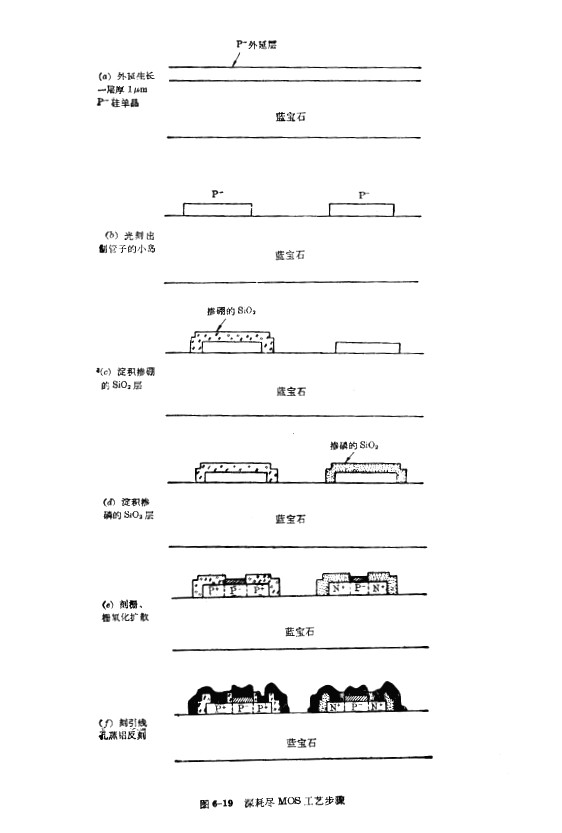
Figure 6-19 shows the main steps of the deep depletion CMOS circuit process. The process is as follows:
①First epitaxially grow a layer on the polished sapphire substrate A P-type silicon layer with a thickness of about 1μm and a resistivity of 10Ω.cm, and a SiO2 protective film is deposited at 400℃ (Figure 6-19 (A)).
②lithography, etching away the silicon layer that is not used as a device , Leaving the epitaxial layer "island" of the tube (Figure 6-19(b)).
③Low temperature fluidized boron-doped SiO2 and then perform photolithography, leaving only the SiO2 layer (pictured 6-
19(c)).
④Low temperature deposition of phosphorus-doped SiO2 and then perform photolithography, leaving only the phosphorus doped at the N channelSiO2 layer (Figure 6-
19(d)).
⑤Engrave the gate to determine the channel regions of NMOS and PMOS respectively .
⑥Gate oxidation and simultaneous boron and phosphorus diffusion. During the gate oxidation process, the boron and phosphorus in the doped oxide diffuse to the two "islands" respectively to form the source and drain regions of the NMOS and PMOS devices (Figure 6-19(e)).
⑦Engrave the lead holes of the source and drain areas.
⑧Steam aluminum, reverse engraving, to form circuit leads (Figure 6 -19(f)).

The right side of Figure 6-19(f) is P+P-P+ The structure is a deep depletion type enhanced work PMOS transistor. The N+P- structure on the left is enhanced Type NMOS transistor. This kind of CMOS circuit has strict requirements on the resistivity and thickness of the epitaxial layer, so the epitaxial layer resistance is required to be high enough to ensure that the P-channel depletion layer is greater than the thickness of the epitaxial layer, but the resistivity cannot be too high. Will make the threshold voltage of the NNOS tube negative. SOS technology manufactures CMOS circuits. But the value of VT of the deep depletion type can be made relatively low, which is its characteristic.
(2)Double epitaxy CMOS process
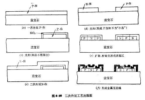
The double epitaxy method is different from the deep depletion type. The NMOS tube is made on the P-type epitaxial layer, and the PMOS tube is made on the N-type epitaxial layer. The N-type epitaxial layer and the upper-type epitaxial layer are epitaxially grown on sapphire twice. The specific process steps are as follows:

①Epitaxially grow a layer of P-type silicon on sapphire Single crystal, etch away the unused parts, and then deposit SiO2 protective layer (Figure 6-20 (a), (b)).
②Secondary extension, on the film after the first extension, A layer of N-type silicon single crystal is grown again, and the unused parts are also etched away. In this way, two P-type and N-type "islands" are formed (Figure 6-20 (c), (d)).
③Diffusion separately to form source and drain regions of NMOS and PMOS (Figure 6-20(e).
④ engraving lead holes, steaming aluminum, reverse engraving, forming electrodes Lead (Figure 6-20(f)).
This process is more complicated, but since the NMOS tube and the PMOS tube are made on two epitaxial layers, they are independent of each other, so the resistivity requirements can be relaxed.
The foundation of the SOS process is to grow a high-quality silicon epitaxial layer, which is closely related to the material quality and processing of the insulating substrate. The substrate material must match the crystal lattice of silicon, and the substrate single crystal is required to be complete, close to the thermal expansion coefficient of silicon, and easy to process.
Since the single crystal structures of silicon and sapphire are different (the former is a cubic symmetric structure, and the latter is a diamond structure), it is difficult to grow a high-quality silicon epitaxial layer. SOS technology manufactures CMOS circuits. Using spinel with cubic symmetry structure instead of sapphire as an insulating substrate can overcome this difficulty, because the mismatch between spinel and silicon is smaller than that of sapphire, but spinel is difficult to obtain and its mechanical strength is not as good as sapphire.
Contact: Mr. Zou
Tel: 0755-83888366-8022
Mobile: 18123972950
QQ: 2880195519
Address: 5C1, CD Block, Tianji Building, Tian’an Digital City, Chegongmiao, Futian District, Shenzhen
Please search the WeChat official account: "KIA Semiconductor" or scan the picture below to "Follow" the official WeChat official account
Please "Follow" the official WeChat account: provide MOS tube technical assistance


