Electronic Technology Forum
Detailed explanation of NMOS devices and process methods and processes
Double-layer gate processThe processes introduced above all use thermally grown silicon dioxide film as the gate Medium material. The use of silicon dioxide as an insulating medium has its unique advantages. It has an ideal interface contact with silicon, and has good insulation and dielectric properties. Therefore, it is still an ideal insulating protective layer in the current planar process. NMOS process. However, with the increasing requirements for MOS circuits, the shortcomings of the silicon dioxide film have been exposed. For example:
①There are movable sodium ions in the silicon dioxide film. When the temperature rises, it will drift under a certain bias voltage, making the device performance unstable;
②The silicon dioxide film has poor radiation resistance, which affects the channel state and surface mobility of MOS devices due to radiation;
③The positive charge in silicon dioxide will induce negative charge on the silicon surface, and the N-channel MOS tube using silicon dioxide as the gate dielectric is easy to deplete, so it must be made Enhanced type is very difficult;
④Silica itself has many defects and interacts with silicon.
In order to overcome the above shortcomings and improve circuit performance, it was found that silicon nitride (Si3N4) and aluminum oxide (Al2O3) Some characteristics of the film are superior to that of silicon dioxide, so the advantages of silicon dioxide, silicon nitride and aluminum oxide are used to form silicon dioxide-silicon nitride And silicon dioxide-aluminum oxide double-layer gate structure, made of NMOS and MAOS devices, thereby improving and enhancing the performance of the circuit. NMOS process. The following describes the properties of the two films and their applications in MOS circuits.
First, NMOS process
1, Si3N4Advantages
NMOS process uses SiO2-Si3N4 The double-layer structure is used as the gate dielectric process of MOS devices. This process is mainly based on the fact that silicon nitride has more advantages than silicon dioxide and is more modern.
The properties of silicon nitride and silicon dioxide are listed in Table 6-1.

From the above table, we can see that using Si3N4 will have the following advantages;
①Si3N4Large dielectric constant and low surface charge density are advantageous for the manufacture of low-threshold voltage enhanced MOS devices, which are compatible with TTL circuits, and because of the high dielectric constant, the conductivity factor can be improved, which is beneficial to improve integration Spend.
②Since Si3N4< The dielectric strength of /span> is larger than that of SiO2, which helps to improve MOS The withstand voltage of the insulated gate.
③In Si3N4, the mobility of sodium ions is very low, so Si3N 4 can be used as a mask to prevent Na+ from intruding; Si3N4 has high density and strong masking ability, not only can mask Na+, but also a variety of impurities, and has good chemical stability, which is beneficial to improve the device The stability.
2, process flow
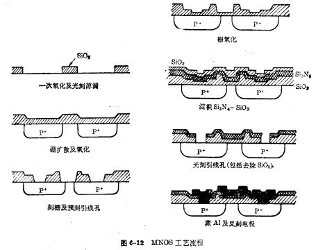
NMOS process is similar to conventional MOS process, except that it has more depositionSi3N4 And corrosionSi3N4 Two process procedures. Take the P-channel enhanced device as an example to illustrate the double-gate SiO2-Si< /span>3N4 The process of structure.
DepositionSi3N4 is performed after gate oxidation. NMOS process. Si3N4 After deposition, another layer of SiO 2, as corrosionSi3N4's masking film. When etching, first etch the SiO2 on the lead hole, and then use a mixture of phosphoric acid mixed with 25% nitric acid at 140℃~160℃ Si3N4 eroded away, and finally the remaining SiO2< /span> Corroded away. As shown in Figure 6-12.

If a 1Ω·cm (100) surface P-type Si substrate is used, the insulating layer uses SiO layer (30nm) and Si3N4 (180nm)
Double-layer dielectric, gate metal A1, can be made into N-channel enhancement type device with NMOS structure.
Contact: Mr. Zou
Tel: 0755-83888366-8022
Mobile: 18123972950
QQ: 2880195519
Address: 5C1, CD Block, Tianji Building, Tian’an Digital City, Chegongmiao, Futian District, Shenzhen
Please search the WeChat official account: "KIA Semiconductor" or scan the picture below to "Follow" the official WeChat official account
Please "Follow" the official WeChat account: provide MOS tube technical assistance


