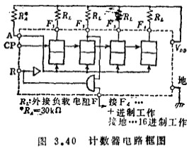
The working principle of the MOS integrated counter circuit diagram The binary flip-flop circuit in the previous section, input a set of "0" and "1" pulses, that is, after inputting a bit of input pul
The working principle of the MOS integrated counter circuit diagram The binary flip-flop circuit in the previous section, input a set of "0" and "1" pulses, that is, after inputting a bit of input pul

MOS integrated flip-flop circuits. In various control instruments and desktop electronic computers, various MOS integrated circuit flip-flop circuits are used. They can be divided into four categories
MOS integrated flip-flop circuits. In various control instruments and desktop electronic computers, various MOS integrated circuit flip-flop circuits are used. They can be divided into four categories

The gate circuit can be considered as a variation of the inverter circuit, basically there are series and parallel modes shown in Figure 3.26. The circuit in Figure (a) is a two-input NOR gate (positi
The gate circuit can be considered as a variation of the inverter circuit, basically there are series and parallel modes shown in Figure 3.26. The circuit in Figure (a) is a two-input NOR gate (positi

MOS integrated inverter circuit, the basis of all circuits-inverter is now explained, as an example of the application of MOS integrated circuits. For ease of description, suppose the form of the tran
MOS integrated inverter circuit, the basis of all circuits-inverter is now explained, as an example of the application of MOS integrated circuits. For ease of description, suppose the form of the tran

An example of a basic circuit for MOS integrated design. Figure 3.20 is a NOR gate circuit composed of P-channel transistors. This circuit adopts the form of leaking ground and is equipped with output
An example of a basic circuit for MOS integrated design. Figure 3.20 is a NOR gate circuit composed of P-channel transistors. This circuit adopts the form of leaking ground and is equipped with output

The advantages of MOS large-scale integration, in addition to the general advantages described in section 3.2.1, there are the following advantages. Compared with bipolar transistors, the manufacturin
The advantages of MOS large-scale integration, in addition to the general advantages described in section 3.2.1, there are the following advantages. Compared with bipolar transistors, the manufacturin
The design of MOS integrated circuits is different from the design of MOS transistors as discrete components. The stray capacitance inside the integrated circuit is small. In order to obtain a certain
The design of MOS integrated circuits is different from the design of MOS transistors as discrete components. The stray capacitance inside the integrated circuit is small. In order to obtain a certain

The function of MOS integrated circuit, amplifying MOS transistor as an active element, is originally used as an amplifying element. In the complementary circuit shown in Figure 3.15, the P-channel an
The function of MOS integrated circuit, amplifying MOS transistor as an active element, is originally used as an amplifying element. In the complementary circuit shown in Figure 3.15, the P-channel an
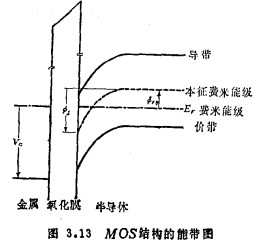
MOS transistor characteristics Integrated circuits are composed of transistors. Therefore, it is desirable for the characteristics of a single transistor to be simple in the design of integrated circu
MOS transistor characteristics Integrated circuits are composed of transistors. Therefore, it is desirable for the characteristics of a single transistor to be simple in the design of integrated circu
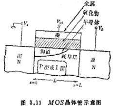
The structure of MOS transistor integrated circuit is an example. Figure 3.12 shows a partial enlarged photo of an N-channel MOS memory large-scale integrated circuit and its corresponding layout patt
The structure of MOS transistor integrated circuit is an example. Figure 3.12 shows a partial enlarged photo of an N-channel MOS memory large-scale integrated circuit and its corresponding layout patt


5C1, CD Block, Tianji Building, Tianan Digital City, Futian District, Shenzhen

KIA-The Public