Electronic Technology Forum
Detailed explanation of AMOS process method and basic flow
1. Main features of AI2O3
AMOS The process is using SiO2-AI span>2O3 Double-layer structure is used as the process of MOS device gate dielectric. The use of this process is mainly based on AI2O3Compared to SiO2 has many advantages. AMOScraft. It can be summarized into three main features:
①AI2O3< /span>The film contains negative charges, so the use of SiO2 A composite structure with a certain thickness ratio can compensate for each other's charges, greatly reduce the equivalent surface charge density, and even drop to zero. It can be used as an effective method to control the threshold voltage of MOS devices, and is particularly suitable for making N-channel enhancement type MOS devices.
②AI2O3< The relative dielectric constant of /span> is 8~10, which is better than SiO2 Is larger, so the double-layer grid with the same thickness can get better than a single SiO2The larger gate capacitance increases the transconductance to increase the switching speed of the circuit.
③AI2O3< /span> has stronger radiation resistance.
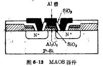
Figure 6-13 shows the N-channel enhanced typeAMOS device. The substrate is (100) P-type single crystal with a resistivity of 8~10Ωcm. The sheet resistance of phosphorus diffusion in the source and drain regions is 4~8Ω/port, on the gateSiO2The layer is grown in dry oxygen, the thickness is 25mm, AI2O 3 The film thickness is about 150nm. In AI2O3< /span> Use low temperature to deposit a layer of SiO2, the thickness is about 500nm. The VT of the manufactured device is 0.5~1.5V, and the field threshold voltage of the field area is above 20V.
2, AMOS process flow
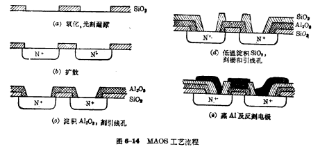
Here is N channelAI< span style="font-size: 10px;">2O3 technology as an example. Figure 6-14 means AMOS process flow chart.


During the process, AI2O3 The corrosion of span> is generally carried out in hot phosphoric acid at 80~85C, and the corrosion rate is 150nm/
min~200nm/min.
Practice shows that AI2O3-SiO2, the polarity of the charge in the double-layer film The performance is related to the conditions of the deposition process, which can be positively or negatively charged, and is also related to the low-temperature annealingconditions.
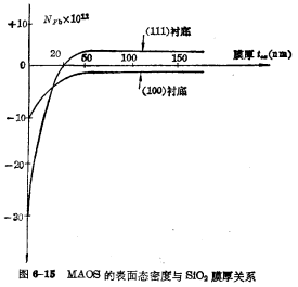
In this case, you can choose from AM OS structure of the flat belt interface charge density Nn and SiO2 membrane dependency to explain.
 < /span>
Figure 6-15 shows AMOS structure and SiO2The film thickness relationship curve. AMOScraft. It can be seen from the graph that the charge density in the AMOS structure And silicon substrate crystal plane index andSiO2 film thickness related. When SiO2 the film thickness is less than20nm,AMOS always with Negative charge, for SiO2 is thicker, such as
  >20nm, the flat-band charge density will be a constant value, and its charge polarity is related to the crystal orientation of the substrate. If the substrate is a (111) plane, the flat-band charge density is positive. If the substrate is a (100) plane, the flat-band charge is always negative.
Contact: Mr. Zou
Tel: 0755-83888366-8022
Mobile: 18123972950
QQ: 2880195519
Address: 5C1, CD Block, Tianji Building, Tian’an Digital City, Chegongmiao, Futian District, Shenzhen
Please search the WeChat official account: "KIA Semiconductor" or scan the picture below to "Follow" the official WeChat official account
Please "Follow" the official WeChat account: provide MOS tube technical assistance


