The so-called ideal MOS tube assumes that there is no positive charge in the gate oxide layer, and electrons cannot be exchanged between the metal gate and the semiconductor (that is, the contact pote
The so-called ideal MOS tube assumes that there is no positive charge in the gate oxide layer, and electrons cannot be exchanged between the metal gate and the semiconductor (that is, the contact pote
The threshold voltage of the MOS field effect tube is the turn-on voltage VT for the enhanced tube, and the pinch-off voltage VT for the depletion tube, which is also denoted by VT for convenience.
The threshold voltage of the MOS field effect tube is the turn-on voltage VT for the enhanced tube, and the pinch-off voltage VT for the depletion tube, which is also denoted by VT for convenience.
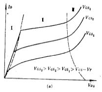
The characteristic curve of MOS field effect tube is discussed with n-channel enhancement mode MOS tube as an example. MOS field effect tube has a variety of connection methods in applications, the mo
The characteristic curve of MOS field effect tube is discussed with n-channel enhancement mode MOS tube as an example. MOS field effect tube has a variety of connection methods in applications, the mo
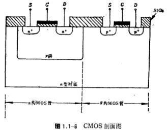
The type of MOS field effect tube. This tube uses n-type semiconductor as the substrate material, and the source and drain regions are p+ diffusion regions. In Figure 1.1-3, replace n+ with p+, and p-
The type of MOS field effect tube. This tube uses n-type semiconductor as the substrate material, and the source and drain regions are p+ diffusion regions. In Figure 1.1-3, replace n+ with p+, and p-
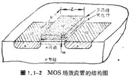
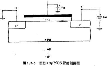
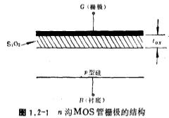
The working principle of the MOS field effect tube, the typical structure of the MOS field effect tube made by the planar process is shown in Figure 1.1-2, where the substrate material is a p-type sem
The working principle of the MOS field effect tube, the typical structure of the MOS field effect tube made by the planar process is shown in Figure 1.1-2, where the substrate material is a p-type sem
The basic principles of MOS field effect transistors. Generally, quality transistors can be divided into two categories. One is called "bipolar" transistors. When this type of transistor works, electr
The basic principles of MOS field effect transistors. Generally, quality transistors can be divided into two categories. One is called "bipolar" transistors. When this type of transistor works, electr
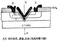
(1) A silicon dioxide mask is grown on the N- epitaxial layer with (100) plane N+-Si as the substrate by one-time oxidation. As shown in Figure 6-26(a). (2) Photolithography, boron diffusion and boron
(1) A silicon dioxide mask is grown on the N- epitaxial layer with (100) plane N+-Si as the substrate by one-time oxidation. As shown in Figure 6-26(a). (2) Photolithography, boron diffusion and boron
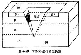
Detailed explanation and analysis of VMOS process structure and characteristics. With the increasing development of MOS large-scale integrated circuits and very large-scale integrated circuits, how to
Detailed explanation and analysis of VMOS process structure and characteristics. With the increasing development of MOS large-scale integrated circuits and very large-scale integrated circuits, how to
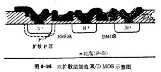
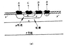
Double-diffusion method for manufacturing E/DMOS double-diffusion method, referred to as DMOS process. The substrate uses P-silicon wafers (called χ substrates). Such a low-concentration P-type substr
Double-diffusion method for manufacturing E/DMOS double-diffusion method, referred to as DMOS process. The substrate uses P-silicon wafers (called χ substrates). Such a low-concentration P-type substr
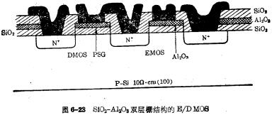
SiO2-AI2O3 double-gate E/DMOS, because the AI2O3 layer contains negative charges, it can offset the positive charges in SiO2, so the thickness ratio of SiO2 and AI2O3 can be controlled, so that the th
SiO2-AI2O3 double-gate E/DMOS, because the AI2O3 layer contains negative charges, it can offset the positive charges in SiO2, so the thickness ratio of SiO2 and AI2O3 can be controlled, so that the th


5C1, CD Block, Tianji Building, Tianan Digital City, Futian District, Shenzhen

KIA-The Public