Electronic Technology Forum
P-channel silicon gate multi-product process flow and its layout design
Silicon gate process" is a process that uses doped polysilicon to make the gate electrode of the MOS tube. The difference from the conventional aluminum gate process described above is that the silicon wafer A thin silicon dioxide layer (gate dielectric) is grown on top, then a thin layer of polysilicon of about 500nm is deposited, and then the source and drain diffusion regions are carved out for source and drain diffusion. P-channel silicon gate process. "Silicon gate process "Compared with the conventional aluminum gate process, it has more characteristics for the performance of devices and integrated circuits.
1. P-channel silicon gate process flow
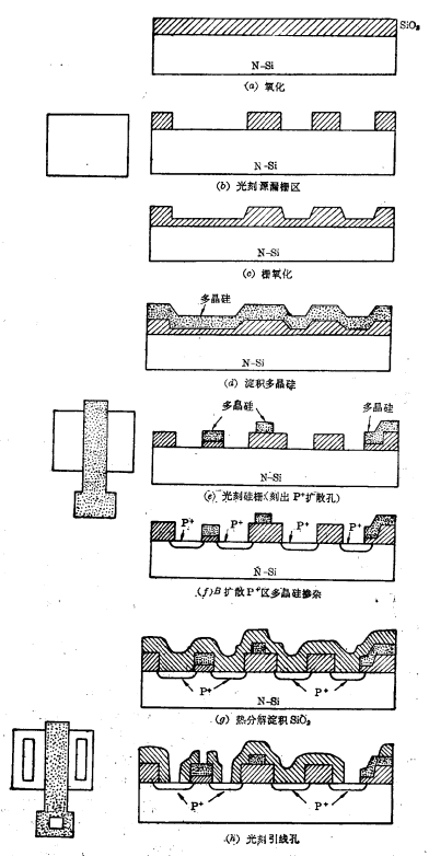
(1) Once oxidation
After the polished Si-type film (5~8Ω·cm) is cleaned, a dry-wet-dry oxidation process is used to grow 1μm SiO2 layer. Such a thick oxide not only serves as a diffusion mask, but also serves as the final field oxide, which is beneficial for reducing parasitic channels.
(2) Lithography source and drain, gate area window (P area)
After photolithography, cleaning process, and then gate oxidation, grow 100~120nmthin SiO The 2 layer constitutes the gate dielectric of the MOS tube.
(3) Precipitated polysilicon
The deposition thickness is 0.4~0.5μm. Electron beam evaporation can be used to deposit polysilicon, or silane thermal decomposition can be used to deposit polysilicon (ie, CVD technology).
(4) Reverse engraving grid
Determine polysilicon patterns, including silicon gates and doped silicon interconnects. There is no registration problem in this lithography. Because the inverted gate determines both the gate area and the source and drain areas.
(5) Boron diffusion
After cleaning, the film with the silicon phase pattern engraved can be expanded and expanded (diffusion source and drain area, P+The interconnect area and silicon gate are heavily doped). P-channel silicon gate process. Since the silicon gate electrode covered on it can be used as a diffusion mask to prevent the channel region from being doped, the source and drain regions of each tube can be automatically aligned with the gate.
The diffused junction depth is<1μm, and the R□ of the silicon gate is 50~100Ω/port.
(6) Low-temperature deposition of SiO2
After removing the borosilicate glass layer, perform low temperature depositionSiO2 , temperature 250~400℃, thickness 300~500nm. The reason why low-temperature deposition is used is to avoid a decrease in sheet resistance after redistribution. The low-temperature silane oxidation method is usually used, and the thermal decomposition method of ethyl orthosilicate can also be used. P-channel silicon gate process.
For passivation, deposit SiO2 , you can proceed with confirmation.
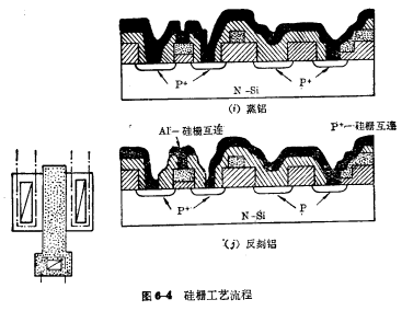
(7) Lithography lead hole
The photo-etched lead holes provide source and drain and metal contacts. After the aluminum is evaporated, the electrodes are reversely engraved to determine the Al interconnection pattern.
The process flow is shown in Figure 6-4.
2, P-channel silicon gate multi-product process
The most important thing in the silicon gate process is the polysilicon process, which is the preparation of polysilicon films as gate electrodes and interconnect lines. Evaporation or sputtering methods are usually used, and thermal decomposition methods of silane (ie, CVD methods) can also be used.
(1) Deposition of polysilicon
If the polysilicon is evaporated by electron beam, in order to make the evaporated silicon film and SiO2 , it adheres well, and the substrate should be kept at 300℃. The typical deposition rate is 300nm/min. Depositing polysilicon requires 0.4~0.6μm, electron beam evaporation can provide a clean and uniform silicon film. P-channel silicon gate process. If the rack for placing silicon wafers adopts a planetary rotating device, the defect of step breakage can be overcome. There is also a problem with electron beam evaporation. The upper part of the evaporation source melts while the bottom part is not. This uneven heating will cause silicon droplets to splash on the wafer and cause large particles. To overcome this shortcoming, the evaporation temperature and rate should be controlled.
High-frequency sputtering can also be used to obtain a uniform silicon layer, but sputtering does not have an electron beam to evaporate cleanly, and there will be heavy ion contamination.


Another method is to use silane to thermally decompose and deposit silicon at 600~750℃. The cleanliness and uniformity of the silicon layer obtained by this method is between evaporation and sputtering. However, polycrystalline silicon is not amorphous like evaporated silicon, but is granular. The size of the particles depends on the growth conditions.
The chemical reaction formula is as follows:

(2) Multi-product silicon corrosion
Polysilicon etching is also an important step in the silicon gate process. The silicon gate process must strictly control the size of the silicon gate, and the width-to-length ratio of the device is largely dependent on the control of the silicon gate size, so the etching conditions for polysilicon are very particular.
Etching polysilicon is usually used Corrosive liquid. P-channel silicon gate process. In order to get a good control, it is best to use a lower corrosion solution. The ratio of HF and HNO2 in the solution depends on the thickness of the polysilicon to be etched. .
Si's anisotropic etchant can also be used for polysilicon. Such as ethylenediamine-H2O series (without phosphoquinol), or ethylene diamineAmine (180cm2)-phosphorusbenzene Diphenol (30g)-pure water (80cm2), temperature 110℃. The corrosion rate for boron-doped polycrystalline silicon is  , 1.4μm/min for undoped polycrystalline, 2μm for phosphorus-doped polycrystalline /min.
Contact: Mr. Zou
Tel: 0755-83888366-8022
Mobile: 18123972950
QQ: 2880195519
Address: 5C1, CD Block, Tianji Building, Tian’an Digital City, Chegongmiao, Futian District, Shenzhen
Please search the WeChat official account: "KIA Semiconductor" or scan the picture below to "Follow" the official WeChat official account
Please "Follow" the official WeChat account: provide MOS tube technical assistance


