Describe the detailed analysis of the high-frequency gain and stability function of the MOS tube. Here, the function derived from the four-terminal parameter as the standard for high-frequency amplifi
Describe the detailed analysis of the high-frequency gain and stability function of the MOS tube. Here, the function derived from the four-terminal parameter as the standard for high-frequency amplifi

The measurement of the estimated MO(y) parameter is used as a circuit design method, and the method of y parameter is generally adopted. In particular, due to the high input impedance of the field eff
The measurement of the estimated MO(y) parameter is used as a circuit design method, and the method of y parameter is generally adopted. In particular, due to the high input impedance of the field eff

The high frequency characteristics of MOS tube structure are improving year by year, and its practical frequency has been extended to very high frequency and even ultra-high frequency. Generally speak
The high frequency characteristics of MOS tube structure are improving year by year, and its practical frequency has been extended to very high frequency and even ultra-high frequency. Generally speak

Charge transfer, charge transfer phenomenon analysis, consider the minority carriers accumulated under the substrate-holes under MOS diode I, add a pulse for charge transfer to the adjacent MOS diode
Charge transfer, charge transfer phenomenon analysis, consider the minority carriers accumulated under the substrate-holes under MOS diode I, add a pulse for charge transfer to the adjacent MOS diode

Charge-coupled devices now have two MOS diodes next to each other as shown in Figure 1.21. Assume that holes injected in a certain method are accumulated under the electrode 1 to form an inversion lay
Charge-coupled devices now have two MOS diodes next to each other as shown in Figure 1.21. Assume that holes injected in a certain method are accumulated under the electrode 1 to form an inversion lay

The MOS diode, assuming a MOS diode, is composed of evaporating aluminum and other metals on a silicon dioxide film grown on N-type silicon, as shown in Figure 1.19. For the sake of simplicity, only t
The MOS diode, assuming a MOS diode, is composed of evaporating aluminum and other metals on a silicon dioxide film grown on N-type silicon, as shown in Figure 1.19. For the sake of simplicity, only t

The noise in MOS field effect transistors includes thermal noise and flicker noise. Thermal noise is inevitable in nature. Flicker noise can be eliminated in principle. However, in actual devices, fli
The noise in MOS field effect transistors includes thermal noise and flicker noise. Thermal noise is inevitable in nature. Flicker noise can be eliminated in principle. However, in actual devices, fli
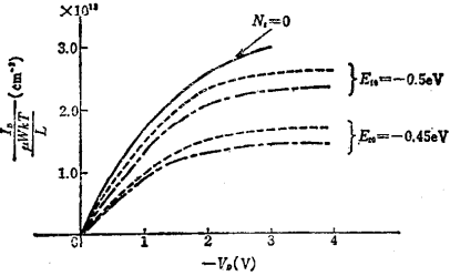
The influence of the static characteristics of MOS field effect transistors, the analysis of the influence of the interface trapping center on the static characteristics of MOS field effect transistor
The influence of the static characteristics of MOS field effect transistors, the analysis of the influence of the interface trapping center on the static characteristics of MOS field effect transistor

Analysis of the characteristics near the threshold voltage of the MOS transistor circuit. The characteristics near the threshold at which the channel current changes from the pinch-off state to the on
Analysis of the characteristics near the threshold voltage of the MOS transistor circuit. The characteristics near the threshold at which the channel current changes from the pinch-off state to the on

The relationship between the carrier mobility and the drain voltage at the interface of the MOS field effect transistor. Under a low electric field, the drift velocity of electrons υd is proportional
The relationship between the carrier mobility and the drain voltage at the interface of the MOS field effect transistor. Under a low electric field, the drift velocity of electrons υd is proportional


5C1, CD Block, Tianji Building, Tianan Digital City, Futian District, Shenzhen

KIA-The Public