Electronic Technology Forum
There are two analysis methods for estimating the high frequency parameters of MOS field effect transistors
There are two methods for estimating the high-frequency parameters of MOS field effect transistors. One is to use four-terminal parameters such as Y or S parameters, and the other is to synthesize and estimate four-terminal parameters from device parameters. The former is rigorous, but the measurement is complicated. The latter is easy to measure, and sometimes it can predict the frequency characteristics of the parameters and the relationship with the offset, but it is not rigorous enough. It is recommended that users refer to the four-terminal constant value published by the manufacturer and appropriately add some measurements within the scope of use.
●) The noise figure of the mixer is also approximately the same order of magnitude (about 1dB difference). In addition, the theoretical value of
 。
。
This value is close to gis in the high frequency band and larger than gis in the low frequency band.
(1) Measurement of y parameter
As a circuit design method, the y parameter method is generally used. In particular, due to the high input impedance of the field effect transistor, it is easy to meet the measurement conditions of input and output short circuits. It can be said that this design method is very appropriate. The following instruments are suitable for measuring Y parameters.
(I) General radio
General Radio's 1607-A transfer function and admittance impedance bridge (TI instrument)
This is a bridge that can measure h, g, y, and z parameters using adjustable-length coaxial cables. It was once widely used to measure the quality of transistors, but the production of this bridge was stopped in 1970. This kind of bridge is also suitable for measuring the Y parameter of field effect transistors. It can measure the transfer admittance of 0-600 in the 25~1500MHz frequency band.0~400
  the input and output admittance values. The measurement accuracy is not high, about 0.1~0.05m3. For smaller values, especially for feedback admittance at low frequencies, devices with smaller input and output admittance values are prone to errors. For complex gate field effect transistors, when the second gate is also biased, there is only a wiring method shown in Figure 2.16 in the TO-5 package package, which is in line with the current standard for cascaded MOS field effect transistors. The output pin wiring method is different, and it is inconvenient for general users, especially in the high frequency band above 100MHz.
(Ii) Heller-Paka
Hewlett Packard's 250 B RX instrument is a two-end electric bridge, which can only measure the input and output admittance, but it is easy to use. The parallel resistance of 15Ω~100kΩ and the parallel capacitance of -80~+20pF can be measured under the frequency of 0.5~250MIHz, and the adapter 13510A for TO-18 and TO-72 shells is attached according to the standard electrode connection, which is convenient Measure the yib, yie, and yoe of the transistor.
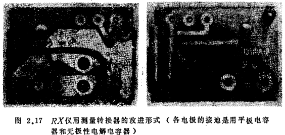
When measuring the parameters of field-effect transistors, the adapter used for measuring yib can be modified to make a multi-purpose adapter as shown in Figure 2.17.
When using the RX instrument, the transfer parameters can be derived from the device parameters such as gm, Crs, and the theoretical formula of the high-frequency parameters described on page 52. However, this method is generally limited to the range below the cut-off frequency of gm.

(2) Measurement of s parameter
The transmission line whose characteristic impedance Z0 is usually a positive real number is connected to the input and output of the device. The so-called s parameter or scattering parameter is a set of parameters when the four-terminal characteristic is expressed by the ratio of the power wave under the Z0 terminal. This kind of measurement does not require open circuit and short circuit conditions that are difficult to achieve at high frequencies. Because there is no or very little possibility of the components that are often problematic under open circuit and short circuit conditions, oscillating, s-parameters have been mainly used in the microwave field in recent years.
In the representation of the s parameter, the independent variables are the incident power wave a1 incident on the input port 1 and the incident power wave a2 incident on the output port 2. The relationship between these independent variables and terminal voltage, current and Z0 can be expressed by the following formula (refer to Figure 2.18)


The dependent variables are the reflected waves b1 and b2

The relationship between the s parameter and the above quantities can be expressed as

Like the Y parameter, it is denoted as S11→Si, S12→ST, S21→Sf, S22→SQ, and the ground angle is usually added (Note ●). From the above formula, the meaning of the s parameter can be obtained as follows:
S11 is the reflection coefficient at the input
S21 is the forward transmission coefficient s21 is the reverse transmission coefficient
S22 is the reflection coefficient at the output
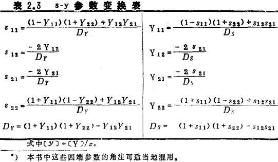
The conversion between s parameter and y parameter is carried out according to the formula in Table 2.3. In addition, there is also a circuit design method that directly uses s parameter 6).

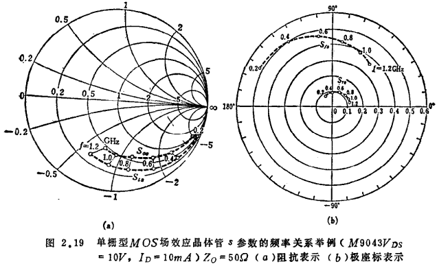
The graphical method of the S-parameter frequency relationship is shown in Figure 2.19. The transmission coefficient is the radial polar coordinate scaled in dB, or the reflection coefficient is marked on the Smith chart to give the admittance or impedance of each pair of ports.

There are the following types of S-parameter measuring instruments.
(I) Heller-Parker
Heller-Parker's 8405 A vector voltmeter This is an instrument that detects the amplitude ratio and phase difference of two signals and is used to measure the transmission coefficient and reflection coefficient. The frequency range is 1~1000MHz. Because the input and output reflection coefficient below 100MHz is very large, it lacks practicality. In addition, Heller-Parker also produced the 8410S used at 110MHz~12.4GHZ and the 8407A network analyzer used at 100kHz~110MHz. The former is particularly convenient for measuring the s-parameters of transistors. Test racks of TO-5 series or TO-18/TO-72 series (below 2GHz) and stripline (below 12.4GHz) are also used. Because it is directly grounded except for the input terminal and output terminal, it is difficult to use for multiple gate type tubes.
There is a capacitor grounding method when measuring complex gate field effect transistors, as shown in Figure 2.20. In fact, the disadvantage of this connection method is that it is easy to extend the effective length of the grounding.
In terms of network analyzers, computers are also equipped to calibrate and perform parameter conversion and gain-stability calculations.
The automation instrument of 8542 A (110MHz~18GHz) and 8543 A (0.1~110MHz).
(Ii) Rhodes and Swartz
Rohde&Schwarz (Rohde&Schwarz) company ZDU type (30~420MHz) ZDD (300~2400MHz) type z-g graphic instrument.
These are all instruments that display light spots on the Smith chart. There is also a ZW A graph instrument (10~480MHz) with a cathode ray tube display capable of frequency scanning measurement. The test frame attached to these instruments is for standard transistors, which is not convenient for measuring complex gate MOS field effect transistors.
(3) Measurement method of high-frequency device parameters 7
As shown on page 52, it is possible to calculate the four-terminal parameters of the device parameters through simple measurements, so it is especially suitable for high-frequency bands.
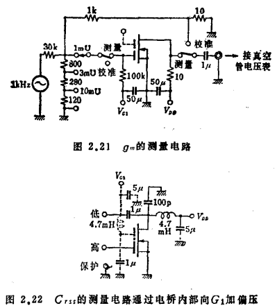
As mentioned on pages 63 to 65, since the input and output admittances are easy to measure, the transconductance gm and the feedback capacitance CTS, which characterize the mutual characteristic relationship, become important parameters. gm (or |Yfs|) can be measured by comparing the input and output voltages under the frequency of use with the structure shown in Figure 2.21.
The measurement of CTS adopts a three-terminal capacitive bridge (Boonton's 76D S8, etc.) equipped with a shielding electrode, and uses the circuit shown in Figure 2.22 to measure within the easy-to-measure frequency range of 0.3~3MHz. The internal gate bias of this circuit is supplied internally through the bridge. In order to suppress leakage oscillation, a capacitor must be bypassed. The total bypass capacitance and lead inductance effectively cause series resonance at the measurement frequency. The inductance and distributed capacitance that play a blocking role effectively resonate in parallel.

Contact: Mr. Zou
Contact number: 0755-83888366-8022
Mobile phone: 18123972950
QQ: 2880195519
Contact Address: 5C1, Block CD, Tianji Building, Tianan Digital City, Chegongmiao, Futian District, Shenzhen
Please search WeChat official account: "KIA Semiconductor" or scan the following picture to "Follow" official WeChat official account
Please "follow" the official WeChat account: provide MOS tube technical assistance


