Electronic Technology Forum
Numerical solution and detailed analysis of charge transport phenomenon
Now consider the case where the minority carriers of the substrate accumulate under the MOS diode I—holes, and a pulse for charge transfer is applied to the adjacent MOS diode II to make the holes transfer from the MOS diode I to II. . Since a pulse for charge transfer is applied to the MOS diode I, there is almost no electric field directed to the MOS diode II in the inversion layer under the MOS diode I, but equivalently, holes are accumulated under the MOS diode I The wall of the potential well is lowered correspondingly in the part adjacent to the MOS diode II. Therefore, the motive force of hole transport is due to the field of mutual repulsion between holes and the diffusion caused by the uneven distribution of holes in space.
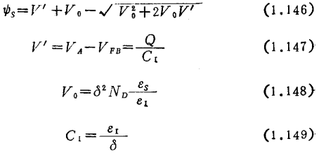
Assuming that the carriers in the inversion layer are concentrated on the interface and are distributed in a δ function, if the remaining space charge layer is approximated as a depletion layer, the interface potential ψs between silicon and silicon dioxide and the external voltage VA have the following relationship:

Where
VFB is the flat band voltage of the MOS diode
Q is the surface charge density of carriers present at the interface
δ is the thickness of the silicon dioxide film
ND is the impurity concentration of the silicon substrate
ξ1 is the dielectric constant of silicon dioxide
ξs is the dielectric constant of silicon
And the current equation is

In the formula, χ is the coordinate from MOS diode I to II
These formulas can be solved simultaneously.
To simplify the problem as much as possible, first linearize the equation (1.146)

The above formula is indeed a pretty good approximation. In addition to the value obtained by the differential equation (1.152), the electric field Ex along the silicon surface also has a part caused by the mutual repulsion of carriers. If the mirror image force generated by the metal gate electrode is also considered, the electric field ER (χ) generated by the mutual repulsion between carriers can be expressed as

result

If the two ends of the MOS diode I are set to x=0 and x=L, the simple boundary conditions are

An example of numerical calculation under this boundary condition is shown in Figure 1.2415). At the beginning of the transfer, the transfer speed at SQ0=2V is 5 times different from that at SQ0=10V, which means that the charge transfer at the beginning of the transfer is caused by the repulsive force caused by the space charge to make the carriers drift, and the transfer speed at the end of the transfer is changed by Proliferation.
Such a process can also be analyzed semi-quantitatively. Substituting formula (1.154) and (1.155) into formula (1.156), we get


Consider that at the beginning of the transmission, , the above formula can be simplified as

At the same time, it is assumed that the distribution of Q is linear

Where Qo is the total amount of holes accumulated in the MOS diode I at each time, so there is

On the other hand, integrate equation (1.150) from x=0 to x=L, and notice that Jp(0)=0, then

which is

If you use equation (1.161) to find Jp(L), the result is 0, so use value infers the value of Jp(L), so there is

Q00 is the starting value of Q0
It can be seen from the above that the more the initial charge is. The faster the transfer of charge.
At the end of the transmission when, the formula (1.158) becomes

This formula is a pure diffusion equation, and its solution is

Q00 is the value of Q0 when t=t', and t'is the time when the transmission speed changes to diffusion control in principle. For convenience, when determining t', take the time when Q0 given by equation (1.164) and Q0 given by equation (1.167) are connected without abrupt change.
At present, charge-coupled devices are under rapid development. Charge-coupled devices are being studied from various aspects, such as improving their use methods, such as reducing the number of phases, improving transmission efficiency, and adding bias charges.
Contact: Mr. Zou
Contact number: 0755-83888366-8022
Mobile phone: 18123972950
QQ: 2880195519
Contact Address: 5C1, Block CD, Tianji Building, Tianan Digital City, Chegongmiao, Futian District, Shenzhen
Please search WeChat official account: "KIA Semiconductor" or scan the following picture to "Follow" official WeChat official account
Please "follow" the official WeChat account: provide MOS tube technical assistance


