The relationship between the carrier mobility at the interface and the gate voltage is so far, the carrier mobility in the channel μch has not been involved too much, and it is regarded as a constant.
The relationship between the carrier mobility at the interface and the gate voltage is so far, the carrier mobility in the channel μch has not been involved too much, and it is regarded as a constant.
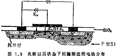
Analysis of the working state of MOS field effect transistor after pinch-off, as explained in the previous section, the limit of the theoretical formula for the area after pinch-off is: the leakage co
Analysis of the working state of MOS field effect transistor after pinch-off, as explained in the previous section, the limit of the theoretical formula for the area after pinch-off is: the leakage co

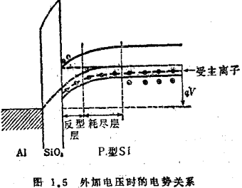
MOS field effect crystal space charge region, the analysis of the space charge formed by impurity ions in the substrate The previous section ignored the space charge 2 formed by impurity ions in the s
MOS field effect crystal space charge region, the analysis of the space charge formed by impurity ions in the substrate The previous section ignored the space charge 2 formed by impurity ions in the s
The working principle of MOS field effect transistor is divided into the discussion of the working principle of MOS field effect transistor. We assume that it has a simple structure as shown in Figure
The working principle of MOS field effect transistor is divided into the discussion of the working principle of MOS field effect transistor. We assume that it has a simple structure as shown in Figure

The working principle of MOS field effect transistors is to apply a voltage of appropriate polarity between the metal electrode of the MOS diode and the silicon substrate. For example, when a P-type s
The working principle of MOS field effect transistors is to apply a voltage of appropriate polarity between the metal electrode of the MOS diode and the silicon substrate. For example, when a P-type s

Switched capacitor full wave detector and peak detector, using switched capacitor circuit to form full wave detector and peak detector, the former is to transform the input signal Vin (t) into its abs
Switched capacitor full wave detector and peak detector, using switched capacitor circuit to form full wave detector and peak detector, the former is to transform the input signal Vin (t) into its abs
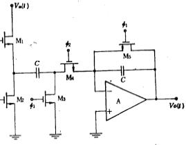
The working principle of the modulator circuit When the amplitude of the carrier frequency signal Vc(t) is positive, M7 and M8 are turned on, the clock signal added to the gate of M1 is ф1, and the cl
The working principle of the modulator circuit When the amplitude of the carrier frequency signal Vc(t) is positive, M7 and M8 are turned on, the clock signal added to the gate of M1 is ф1, and the cl
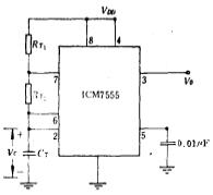
ICM7555 internal circuit diagram, ICM7555 time base internal circuit diagram and its function analysis The internal circuit diagram of ICM7555 is shown in Figure 6.3-2. Corresponding to Figure 6.3-1,
ICM7555 internal circuit diagram, ICM7555 time base internal circuit diagram and its function analysis The internal circuit diagram of ICM7555 is shown in Figure 6.3-2. Corresponding to Figure 6.3-1,

The time base circuit is a timing circuit, which generates a pulse with a fixed time width under the action of a trigger pulse. The time width is determined by the timing resistor and the timing capac
The time base circuit is a timing circuit, which generates a pulse with a fixed time width under the action of a trigger pulse. The time width is determined by the timing resistor and the timing capac

Switched capacitor sine oscillator, a sine oscillator composed of a double second-order switched capacitor circuit (Figure 5.3-12c) is shown in Figure 6.2-3. The op amps A1, A2 and capacitors CA, CB,
Switched capacitor sine oscillator, a sine oscillator composed of a double second-order switched capacitor circuit (Figure 5.3-12c) is shown in Figure 6.2-3. The op amps A1, A2 and capacitors CA, CB,


5C1, CD Block, Tianji Building, Tianan Digital City, Futian District, Shenzhen

KIA-The Public