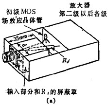
MOS field effect transistor weak voltage amplifier circuit 56) 57) If the signal source resistance Rs is 100MΩ, the change part of Ig is 1×10-14A, and the drift voltage generated by the gate current I
MOS field effect transistor weak voltage amplifier circuit 56) 57) If the signal source resistance Rs is 100MΩ, the change part of Ig is 1×10-14A, and the drift voltage generated by the gate current I
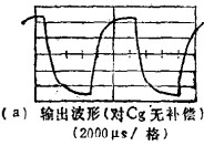
MOS field effect transistor weak current amplifying circuit and measurement method are summarized, the circuit structure usually used for measuring weak current has three types shown in Figure 2.86. I
MOS field effect transistor weak current amplifying circuit and measurement method are summarized, the circuit structure usually used for measuring weak current has three types shown in Figure 2.86. I
The relationship between the DC bias circuit 48) and the operating point. The DC coupling amplifier circuit refers to a circuit in which the input stage, output stage and inter-stage are directly coup
The relationship between the DC bias circuit 48) and the operating point. The DC coupling amplifier circuit refers to a circuit in which the input stage, output stage and inter-stage are directly coup
The DC amplifier circuit is roughly divided into the DC coupling circuit described in section 2.2.2 and the modulation type amplifier circuit described in section 2.2.5. Appropriately giving the high-
The DC amplifier circuit is roughly divided into the DC coupling circuit described in section 2.2.2 and the modulation type amplifier circuit described in section 2.2.5. Appropriately giving the high-
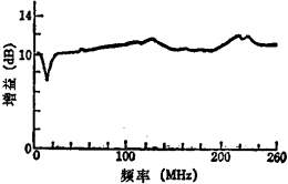
The CR coupling and distributed amplifier of the MOS field effect transistor broadband amplifier are illustrated as examples. The broadband amplifier is also useful for tuning amplifiers (such as the
The CR coupling and distributed amplifier of the MOS field effect transistor broadband amplifier are illustrated as examples. The broadband amplifier is also useful for tuning amplifiers (such as the
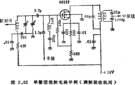
MOS field effect transistor frequency conversion (mixing) circuit MOS field effect transistor frequency conversion (mixing) circuit principle operation and example analysis of square law characteristi
MOS field effect transistor frequency conversion (mixing) circuit MOS field effect transistor frequency conversion (mixing) circuit principle operation and example analysis of square law characteristi
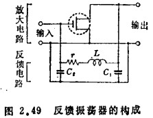
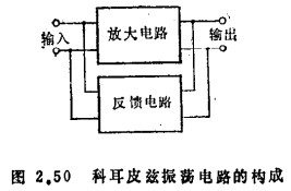
High-frequency oscillation circuit Almost all vacuum tube feedback oscillation circuits can be used in MOS field effect transistor oscillation circuits, and compared with vacuum tubes, MOS field effec
High-frequency oscillation circuit Almost all vacuum tube feedback oscillation circuits can be used in MOS field effect transistor oscillation circuits, and compared with vacuum tubes, MOS field effec
The first use of high-frequency MOS field effect transistors, and currently the most used are the RF stage and the first mixing stage of FM receivers; with the appearance of cascaded transistors, they
The first use of high-frequency MOS field effect transistors, and currently the most used are the RF stage and the first mixing stage of FM receivers; with the appearance of cascaded transistors, they
The role of MOS field effect transistor high-frequency amplifier circuit in the receiving system is (1) to improve the signal-to-noise ratio, (2) to reduce the received clutter signal, and (3) to prev
The role of MOS field effect transistor high-frequency amplifier circuit in the receiving system is (1) to improve the signal-to-noise ratio, (2) to reduce the received clutter signal, and (3) to prev
Design of MOS Field Effect Transistor Bandpass Amplifier 1" For the sake of simplicity, take a single-tuned amplifier circuit as an example, and use the most common y-parameter notation to illustrate
Design of MOS Field Effect Transistor Bandpass Amplifier 1" For the sake of simplicity, take a single-tuned amplifier circuit as an example, and use the most common y-parameter notation to illustrate


5C1, CD Block, Tianji Building, Tianan Digital City, Futian District, Shenzhen

KIA-The Public