Electronic Technology Forum
Detailed analysis of MOS diode's transient response state voltage analysis
Charge coupled device
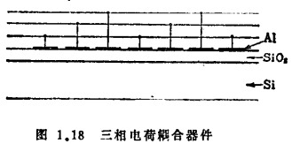
As shown in Figure 1.18, many MOS diodes are arranged on a plane, the charge in the inversion layer is not transferred to the external circuit, and the devices transferred in the adjacent MOS diodes are called charge coupled devices (charge coupled deυices) 13). The essential difference with the MOS field effect transistor is that the carriers in the inversion layer are determined by a signal that has nothing to do with the gate voltage, and the gate voltage has nothing to do with the signal and is only used to transfer charges. As mentioned in the section on the operation of MOS field effect transistors, there must be a one-to-one correspondence between the carrier density in the inversion layer and the gate voltage in the steady state. In order to complete the above work, it must be in the transition Use under state. Therefore, the work of the charge-coupled device is a continuous transition state. Here we first consider the transition state of the MOS diode.

Transition response of MOS diode
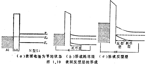
Suppose there is a MOS diode, which is composed of evaporating aluminum and other metals on a silicon dioxide film grown on N-type silicon, as shown in Figure 1.19. For the sake of simplicity, only the gate voltage refers to the effective gate voltage. A zero gate voltage means that the electric field on the silicon surface is zero, as shown in Figure 1.19(a). For example, when a negative voltage is applied to the gate relative to the silicon substrate, when the applied voltage is not too large, a depletion layer is formed on the silicon surface, as shown in Figure 1.19(b); if a larger negative gate voltage is applied, As we all know, an inversion layer is formed on the silicon surface, as shown in Figure 1.19(c). Please note that this is the steady state situation.
Now look at the situation where a large negative pulse voltage is superimposed on the gate voltage. In order to immediately form an inversion layer corresponding to the pulse voltage, a hole current must be injected into the silicon surface to supply the inversion layer with holes. The heat generation of carriers in the space charge layer is very slow. Let τp be the carrier lifetime and ni is the intrinsic carrier density, then the generation rate g is 14)


If the donor concentration in the silicon substrate is ND, the time t0 required to form the inversion layer is

Even if the carrier lifetime is on the order of microseconds, t0 is also on the order of seconds, so the formation of the inversion layer cannot keep up with the pulse voltage anyway. In addition, the possibility of injecting hole current through the ohmic contact of the silicon substrate can also be considered. However, hole current cannot be injected into the N-type semiconductor through the ohmic contact formed by the N N+ junction. As shown in Figure 1.20, there is a barrier at the interface between the metal of the ohmic electrode and the N+ layer. The barrier height is equal to the difference between the work function фM of the metal and the electron affinity χ of silicon, but due to the potential in the N+ layer The thickness of the barrier is very thin, and the conductive electrons in the silicon reach the metal through the tunneling effect, forming a so-called ohmic contact. However, for holes injected from metal to silicon, there will be a very high barrier as shown in Figure 1.20, so there is almost no hole injection.
As a result, when a large negative voltage is applied to the gate of a MOS diode, such as when there is no hole injection source like a MOS field-effect transistor, the hole distribution and thermal balance are not much different, only because the conductive electrons are far away from the only Surface, and the depletion layer formed at the surface of Gui. But over time, this state will change due to the accumulation of thermally generated minority carriers until an inversion layer is formed on the silicon surface.
The formation time of the inversion layer is on the order of seconds as mentioned above. When investigating the phenomenon that occurs in a time shorter than milliseconds, such as adopting a minority carrier injection tunneling method, adding a gate to the gate to make the majority The voltage in such a direction that the carriers are far away from the silicon surface can form an inversion layer on the silicon surface. Such as not taking special measures to inject minority carriers. No inversion layer is formed on the silicon surface.
Contact: Mr. Zou
Contact number: 0755-83888366-8022
Mobile phone: 18123972950
QQ: 2880195519
Contact Address: 5C1, Block CD, Tianji Building, Tianan Digital City, Chegongmiao, Futian District, Shenzhen
Please search WeChat official account: "KIA Semiconductor" or scan the following picture to "Follow" official WeChat official account
Please "follow" the official WeChat account: provide MOS tube technical assistance


