Electronic Technology Forum
A brief description of the charge-coupled device overview process and working principle
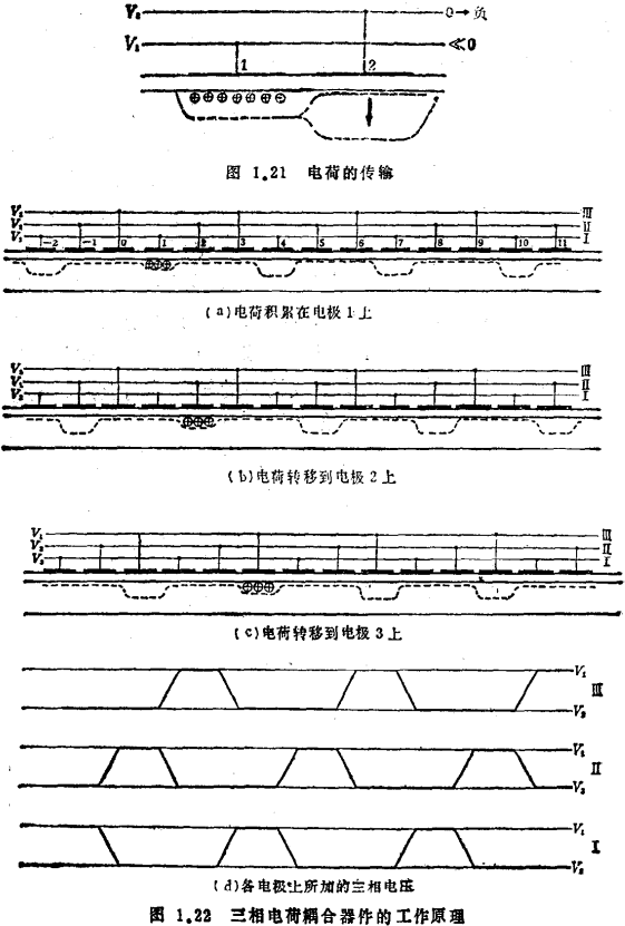
Today there are two MOS diodes in close proximity as shown in Figure 1.21. Assume that holes injected in a certain method are accumulated under the electrode 1 to form an inversion layer. It is also assumed that a voltage is applied to the electrode 2 and its polarity is selected so that a depletion layer is formed under the electrode 2 or an accumulation layer is formed. And suppose that a large voltage of a certain polarity that can form an inversion layer is applied at a certain moment. The two MOS diodes are very close, so that the depletion layer of the MOS diode 2 reaches the inversion layer of the MOS diode 1, and the minority carriers in the MOS diode 1 are transferred to the MOS diode 2 at this time. Therefore, if MOS diode arrays are manufactured close to each other, and voltages are sequentially applied from one side, minority carriers can be transferred sequentially, and circuits such as shift registers, delay lines, and scanning circuits can be simply constructed. Devices made based on the above principles are called charge-coupled devices.

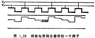
If each MOS diode is independently applied with a voltage, it will increase the number of leads, which is not economical. However, when the transfer direction of minority carriers is one-dimensional, if no special measures are taken on the device itself, a three-phase voltage is used instead. Three leads can ensure the unidirectionality of carrier transfer. As shown in Figure 1.22(a), assuming that there are holes only under electrode 1, apply voltages V1, V2, and V3 to electrodes 1, 2, and 3 respectively. An accumulation layer or a depletion layer is formed in the steady state of the electrode with a voltage of V2. If such voltage conditions are met, the holes under the electrode 1 will not move elsewhere in this state. To this structure, add the time-varying voltage shown in Figure 1.22(d), that is, the voltage of electrode 1 is V2, and the voltage of electrode 2 is V1, and the holes under electrode 1 are transferred to under electrode 2. Similarly, if the voltage of the electrode 2 is Vz and the voltage of the electrode 3 is V1, the holes will be transferred to the electrode 3. If two-phase voltage is used at this time, the same voltage is applied to electrode 1 and electrode 3, and the holes are distributed on electrode 1 and electrode 3. Therefore, three-phase voltage must be applied to keep the voltage of electrode 1 at V2 and electrode The voltage of 3 becomes V1. In the same way, if holes are to be transferred from electrode 3 to electrode 4, the voltage distribution of each electrode must be restored to the initial state where there are holes under electrode 1, so that the charge transfer of one bit is just completed. This is the principle of a three-phase charge-coupled device. In the direction of minority carrier transfer, if an electric field can be applied from the outside with a voltage, or an electric field can be built in, the number of phases of the charge-coupled device can be reduced. Figure 1.23 is an example of a two-phase charge-coupled device.
Contact: Mr. Zou
Contact number: 0755-83888366-8022
Mobile phone: 18123972950
QQ: 2880195519
Contact Address: 5C1, Block CD, Tianji Building, Tianan Digital City, Chegongmiao, Futian District, Shenzhen
Please search WeChat official account: "KIA Semiconductor" or scan the following picture to "Follow" official WeChat official account
Please "follow" the official WeChat account: provide MOS tube technical assistance


