Electronic Technology Forum
Detailed analysis of noise generation mechanism and 1/f noise in MOS field effect transistors
The noise in MOS field effect transistors includes thermal noise and flicker noise. Thermal noise is inevitable in nature. Flicker noise can be eliminated in principle. However, in actual devices, flicker noise or 1/f noise is a representative noise. The noise plays a decisive role. Let's discuss the relatively simple thermal noise first, and then discuss the 1/f noise.
(1) MOS field effect transistor thermal noise
Thermal noise is generated due to the random thermal movement of electrons in the channel, and this thermal noise generates a thermal noise voltage through the resistance in the channel. When calculating the thermal noise current generated from this, it must be noted that the thermal noise voltage will change the channel potential, which is equivalent to a change in the effective gate voltage, and therefore the leakage current also changes.

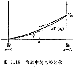
As shown in Figure 1.16, set the distance from the source to the channel as at both ends of the interval
 the voltage fluctuates. Set
 the electric potential fluctuates at
 when, then there is

As an expression showing the relationship between the leakage current and the channel potential of a MOS field effect transistor, the simplest formula (1.13) is used, namely

Because of this potential fluctuations
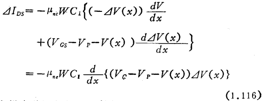
 the fluctuation of leakage current caused by
 can be written as

If the channel length is L, the source is grounded and the output noise current in a short-circuit state is

So that when 


When 

As will the value of is substituted into the formula (1.118) in
 ,will
,will the value of is substituted into the formula (1.119) in
 ,
, of course it becomes the universal value of the entire channel, so

 Conductance per unit length of the channel at
  for
for

 can be written as

So far, did not consider what caused it. When the cause is thermal noise, assume
 the resistance between
 ,
, Is the bandwidth of the researched bandwidth.
Then there is
Then there is

because

then

Thermal noise is not only occurs in the interval, but it will happen in the entire channel area. Now let the noise component of the leakage current be
 ,Using formula (1.115), (1.121), can be written

Where

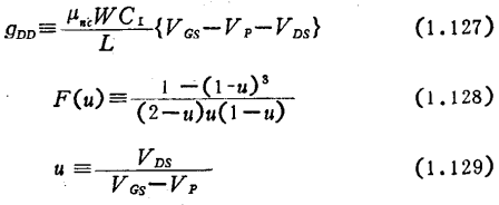
When the leakage voltage is very small, that is, when u→0,

This gives the so-called thermal noise as a resistor. The leakage voltage is very large. When it is close to the pinch-off state, the F(u) value itself tends to infinity, but the gDD value tends to infinitely small, so the noise current output will not increase indefinitely.
(2) MOS field effect transistor 1/f noise
There is a kind of noise component in the low frequency region, and its power spectrum increases roughly inversely proportional to the frequency. It is known from experiments that this kind of noise has significant differences with the surface state. As far as MOS field effect transistors are concerned, the cause of this noise is either because the carriers in the channel are trapped by the interface state, or the carriers in the channel are generated by releasing carriers from the interface state into the channel. The fluctuation of the number of children.
In the trench number of carriers in range
 the fluctuations. assumed
 Channel resistance
 fluctuations, the resulting voltage fluctuations
 for
for

Use relations

available

The reuse formula (1.119) can be deduced

Thus if the power spectral density is
 ,then
,then power spectral density
 for
for

Try below . power spectral density and
 normalized autocorrelation function
 ,
,

There is the following relationship between

This is the familiar Wiener-KhinTchine theorem 11), so the autocorrelation function is first required. Assuming that the probability of carrier generation or recombination per unit time is .R(t) is a function representing the source of random variation, the number of carriers fluctuates from the average
 the change over time can be expressed by Langevin's differential equation as follows.

The phenomenon that occurs at a certain time t continues to time the ratio of can be regarded as the component in formula (1.138) that is not affected by R(t), so it is obviously

Substituting this formula into formula (1.137), we have

The formula (..140) assumes that the fluctuation of dN uses only one time constant the solution of the phenomenon that can be represented. Decide
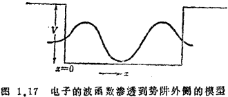
 the physical mechanism of is very complex 12). The simplest model is that the wave function of the electron penetrates the outside of the square wave potential well, as shown in Figure 1.17. In the x direction, the wave function can be expressed as
 ,where
 ,
, Is the effective mass of the electron, V is the depth of the potential well, and E is the electron energy. The electrons are transferred to the trap level in the silicon dioxide film at a distance x from the silicon-silicon dioxide interface through the tunneling phenomenon, and the trapping probability is assumed to be
 ,Then the capture time of this trap energy level can be expressed as

Assume that the spatial distribution density of trap energy levels in the silicon dioxide film is , The noise spectral density when these trap levels exist at the same time
 for
for

 When
When  is uniformly distributed.

The frequency spectrum of 1/f is given. In other words, the so-called 1/f noise generation mechanism, which is related to such a surface, plays a decisive role.
Contact: Mr. Zou
Contact number: 0755-83888366-8022
Mobile phone: 18123972950
QQ: 2880195519
Contact Address: 5C1, Block CD, Tianji Building, Tianan Digital City, Chegongmiao, Futian District, Shenzhen
Please search WeChat official account: "KIA Semiconductor" or scan the following picture to "Follow" official WeChat official account
Please "follow" the official WeChat account: provide MOS tube technical assistance


