Electronic Technology Forum
Analysis of working principle of high frequency characteristics of MOS field effect transistor
The high frequency characteristics of MOS field effect transistors are improving year by year, and its practical frequency has been extended to very high frequency and even ultra-high frequency bands. Generally speaking, compared with bipolar transistors, field-effect transistors have the characteristics of less non-linearity at high frequencies and good large-signal characteristics. Compared with the junction field effect transistor, the MOS field effect transistor has a higher mobility of majority carriers in the channel of the junction transistor, and the MOS field effect transistor has a simple structure, which is conducive to miniaturization. MOS tube structure high frequency. For the single-gate type, the high-frequency characteristics of the two types of field effect transistors can be said to be not much different 1), but in the complex structure of the cascade type, the MOS type is more advantageous, and many products have appeared and are used in various aspects. .
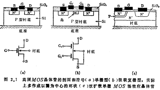
The current high-frequency MOS field effect transistors are roughly divided into two types: single-gate type and cascaded multiple-gate type ●). The former is easy to manufacture due to its simple structure (refer to Figure 2.1(a)), and when the gm is equivalent, the cut-off frequency is higher, but the feedback capacitance is larger; the latter has a more complicated structure (refer to Figure 2.1(b)), and the feedback capacitance is smaller , Because there are two control electrodes, the degree of freedom is increased, which is convenient to adjust the gain, but the cut-off frequency is lower. For high-frequency field effect transistors, in order to make image.png larger, the channel should be made very narrow, and in order to increase gm, the length of the gate must be increased.
●) For single-gate field-effect transistors, both the junction type and MOS type can easily obtain the same order of frequency characteristics. Since the junction type has a stable critical voltage, there is no need to worry about gate damage, and the junction type is better; on the other hand, For the cascade gate type, because of its complex structure, the MOS type is more conducive to miniaturization than the junction type, so it is official to use MOS.
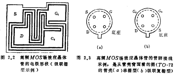
For this reason, the serpentine pattern shown in Figure 2.2 can be used, and the chip area of the cascade gate type is especially to be increased. These high-frequency field-effect transistors are usually packaged in a TO-72 case. MOS tube structure high frequency. Typical pin connections are shown in Figure 2.3.
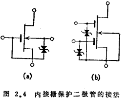
Because the gate insulating film of the MOS field effect transistor is thin and the leakage current is small, the gate is easily charged. Therefore, the gate insulating layer is often damaged due to frictional electrification, electric leakage from the soldering iron, or other impulsive electric pulses. In order to prevent this from happening, a protective diode can be added to the gate so that the gate voltage will not exceed a certain value 2).
Especially for high-frequency applications, two modes of enhancement and depletion are often used, so back-to-back diodes as shown in Figure 2.4 are often used to protect them by the reverse breakdown characteristics of the diodes ●). Recently, the protection diode and the field effect tube body are mostly built on the same chip, that is, the so-called "monolithic" structure is the main one.
Signetics has commercialized double diffused MOS transistors (D-MOS for short). However, the field-effect transistor with essentially the same structure should be said to be the first successfully developed by Tarui et al. in 19693). The basic structure is shown in Figure 2.1 (C) (single gate type). The double diffusion process can automatically determine the narrow channel width, and there is a high resistance drift field area near the drain (there is to increase the drain junction breakdown voltage and reduce the feedback capacitance Role) for its characteristics. MOS tube structure high frequency. Signet produces single-gate (SD200/201) and multiple-gate (cascade, SD300/301) double diffused MOS transistors. SD200 can get 8dBmin gain (MAG) and 4.5dBmax noise figure at 1GHz, while SD301 can get better characteristics such as 10dBmin and 7dBmax respectively.
(1) High-frequency characteristics of single-gate MOS field effect transistors
The structure of the single-gate MOS field effect transistor can be seen in Figure 2.5 (a), and the equivalent circuits corresponding to the source grounding and gate grounding are shown in Figure 2.5 (b) and (c) respectively.
In order to improve the high frequency characteristics, the base can be grounded. The "components" outside the dashed line in the figure are formed by the package and chip leads, and the "components" within the dashed line correspond to the chip part.
●) The potential of the middle junction of the back-to-back diodes sometimes cannot follow the gate voltage for rapid changes. It takes time to discharge the charge at the intermediate node through the reverse of the two diodes. If the electrostatic capacitance of the protection diode cannot be ignored, it will cause transient detuning. Therefore, it is advisable to avoid abrupt changes in the gate voltage.
The y parameter of a MOS field effect transistor can be easily obtained from the equivalent circuit. When the inductance factor is ignored, taking the source ground as an example, the following formulas can be roughly obtained.
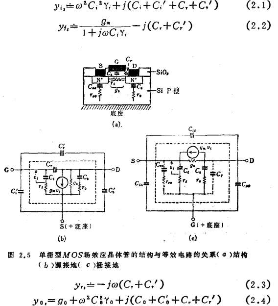
These formulas are in ,
, established when. The device parameters in the formula are defined as follows:
Ci is the gate capacitance, which is a constant value almost independent of the bias voltage.
Ci+Cˊi is the input capacitance
gm is the low-frequency value of the transconductance. Its relationship with bias voltage is

 is the gate resistance, which is the resistance of the channel part seen from the gate, and its value is about
 is the feedback capacitor
go is channel conductance
Co is the leakage junction capacitance (with
Relationship)
Co+Cˊo is the output capacitance
ro is the leakage junction series body resistance
It should be noted that when the gate is grounded, the input conductance of the equivalent circuit in Figure 2.5(C) (only the intrinsic part is considered, Css is omitted) is

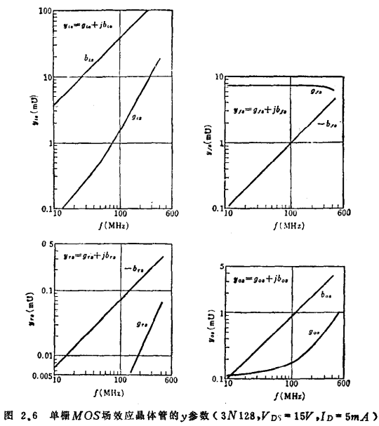
The frequency relationship of the Y parameter when the source of a typical high-frequency single-gate MOS field effect transistor is grounded is shown in Figure 2.6. Obviously shows the frequency-dependent characteristics of the above-mentioned Y parameter, which can also be used to calculate the device parameter value. MOS tube structure high frequency. The maximum usable power gain Gma calculated from Fig. 2.6 and the stability factor of Rollet (Rollet) the value is shown in Figure 2.23. It can be seen that although the feedback capacitance of the MOS field effect transistor is quite small, the stability is not high due to the high input impedance. Therefore, when high gain is desired at high frequencies, neutralization must be performed, which is very inconvenient.
When the junction field effect transistor is used at a higher frequency such as an ultra-high frequency band, the gate ground may be amplified more stably than the source ground. However, for MOS field effect transistors, due to the difference between the source and the background The junction capacitance is added to the input side, which greatly deteriorates the frequency characteristics, so the gate grounding method is usually not adopted at present.
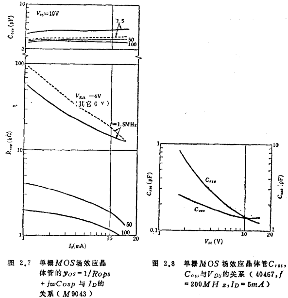
In the dependence of the high-frequency parameters of the single-gate MOS field-effect transistor on the bias conditions, The relationship with the bias is not too big, and can usually be ignored ●) (this point is the same as the cascade gate type). in
 the high frequency band, which is almost unaffected by the channel resistance go, is controlled by Co's compliance with VDS. However, after the frequency is reduced, it will be affected by the compliance of go to ID, and generally has
 relationship (see Figure 2.7). Especially for high-frequency field effect transistors and other devices with low substrate impurity concentration,
 the value is easy to increase. When ID=10mA, its output impedance is in the order of 10-20kΩ. Compared with a transistor, its output impedance is often lower. MOS tube structure high frequency. In addition, we noticed that the higher the VDS, the smaller the go, but it rises sharply near the breakdown voltage (this is also similar to the cascade gate type, see Figure 2.13). When VDS is below 5V,
 It also increased sharply (see Figure 2.8).
●)But in the triode working area or the area with very low current, there is a decreasing trend.
At present, there are not many commercial varieties of single-gate MOS field effect transistors for high-frequency use.
(2) Cascade type complex gate MOS field effect transistor
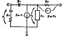
As mentioned above, the high-frequency instability of the single-gate field effect transistor can be improved by the cascode connection. The circuit formed by the cascade connection of the field-effect transistor with the source grounded at the input end and the field-effect transistor with the gate grounded at the output end is shown in Figure 2.9.

Suppose the y parameter of the front-stage field effect transistor is

Then the y parameter of the cascade circuit can be expressed as 4)
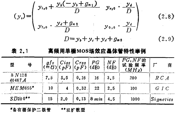
At frequencies much lower than the gm cutoff frequency, the value of gm2 (~gm1) plays a decisive role in D, so ,
, the value can be approximated by the value of the previous stage, and
 ,
, value decreases
. If yc=yb is set, this value becomes 1/(μ2+2), where μ2 is equal to gm2/yd, which is the voltage amplification factor of the post-stage field effect transistor. Therefore, if the rear-stage field effect transistor is in the pentode area, the feedback capacitance is greatly reduced, which is almost equal to the lead capacitance, and the low-frequency output admittance is also reduced. In general, the stability is improved.
●) In the range determined by the drain-body capacitance and the body series resistance, that is, in the area proportional to ω2, the output conductance is the same as the single-gate type.
Due to its high stability and various advantages described below, this type of field effect transistor has been produced for very high frequency applications. MOS tube structure high frequency. Its cross-sectional structure as shown in Figure 2.1 (b) seems to be very simple, but in fact the source-drain spacing is relatively wide, and the actual graph is shown in Figure 2.2, which is quite complicated.
DC characteristics and low frequency characteristics
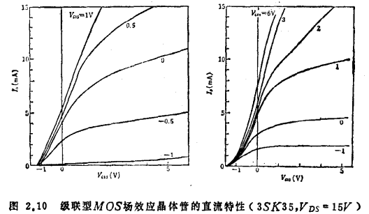
The DC characteristics of the cascaded MOS field effect transistor can be simply synthesized by the DC characteristics of the two field effect transistors. That is, the leakage currents of the two field effect transistors are equal, and the total leakage voltage is the sum of the leakage voltages of the two transistors, and it can be considered that the second field effect transistor is essentially controlled by the gate-island voltage. Because the two tubes are connected in series, even if the gate voltage of one tube increases, the leakage current is limited by the other tube and cannot increase (refer to Figure 2.10).
The relationship between gm and bias voltage can also be derived from the DC characteristics. There is an area that decreases as the leakage current increases (refer to Figure 2.11).
High frequency characteristics
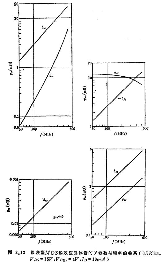
The relationship between the y parameter and the frequency is shown in Figure 2.12. It is similar to the single-gate type in the practical frequency band. Due to the feedback capacitor, that is Greatly reduced, it is possible to carry out stable work (refer to Figure 2.23). Conversely, because the two channels are connected in series, resulting in
 deterioration of frequency characteristics (refer to Figure 2.12).
The relationship between high-frequency parameters and bias is roughly the same as that described in the single-gate section, but the low-frequency  is slightly different.
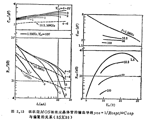
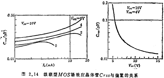
 the value itself is lower than that of the single-gate type. If an excessive bias is applied to the second gate along the depletion direction, then
 increase, the output impedance decreases (refer to Figure 2.13, 2.14).
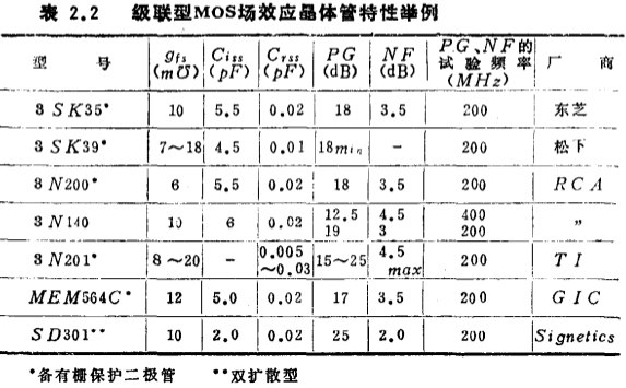
This type of MOS field effect transistor has lower crosstalk modulation characteristics. As shown in Figure 2.35, as the feedback capacitance is reduced, the frequency offset during automatic gain control is also reduced, so the tube may be widely used in the pre-stage of VHF TVs. Its products are shown in Table 2.2. MOS tube structure high frequency. Almost all products are equipped with gate protection diodes, and the practical frequency is 400~500MHz.
(3) High-frequency noise characteristics of MOS field effect transistors 5)
There will be a separate section for details on the noise mechanism and other issues, here we only focus on high-frequency noise. The theoretical formula for the noise figure F of a grounded MOS field effect transistor can be expressed as follows.

where admittance to the signal source
 admittance for the best signal source
 。
。
 equivalent noise resistance
Change the signal source admittance so that (Noise tuning) and
 (Noise matching), the lowest noise figure Fmin can be achieved. usually,
 admittance of signal source at maximum gain
 different. Taking into account the thermal noise of the channel part and the noise induced on the gate electrode, if the correlation between the two noises is ignored, a theoretical formula of Fmin is

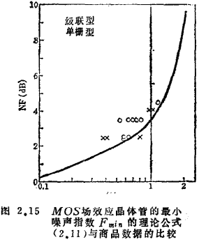
It is determined by the characteristic frequency fo. In addition, in MOS field effect transistors, the noise generated by the interface state can be extended to high frequencies, and there are other parasitic factors, especially for cascaded inter-stage mismatch and other reasons. Generally, the value of Fmin given is higher than the above formula. Big. The formula (2.11) shown in Figure 2.15 is compared with the data of commercially available field-effect transistors to get a rough standard ●).
Contact: Mr. Zou
Contact number: 0755-83888366-8022
Mobile phone: 18123972950
QQ: 2880195519
Contact Address: 5C1, Block CD, Tianji Building, Tianan Digital City, Chegongmiao, Futian District, Shenzhen
Please search WeChat official account: "KIA Semiconductor" or scan the following picture to "Follow" official WeChat official account
Please "follow" the official WeChat account: provide MOS tube technical assistance


