Electronic Technology Forum
Explain the basic working principle and circuit diagram analysis of the modulator in detail
Using MOS switched capacitor technology, some important non-linear circuits (such as modulators, detectors, etc.) can be made into MOS integrated circuits.
1. Modulator circuit diagram
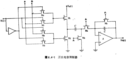
A typical switched capacitor modulator is shown in Figure 6.4-1. In the figure, Vm(t) is the modulation signal, and Vc(t) is the carrier frequency signal. The output signal Vo(t) is the product of Vm(t) and Vc(t). Therefore, the circuit shown in Figure 6.4-1 is also called a multiplier. In order to make the circuit work normally, the frequency of the clock signal ф1 and ф2 should be much greater than the frequency of the carrier frequency signal.
2. The working principle of the modulator circuit
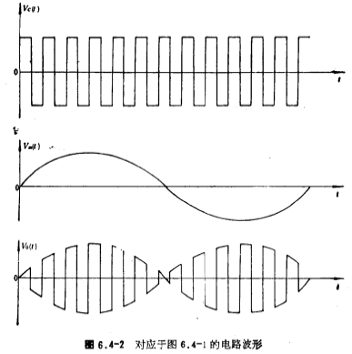
When the amplitude of the carrier frequency signal Vc(t) is positive, M7 and M8 are turned on, the clock signal applied to the gate of M1 is ф1, and the clock signal applied to the gate of M1 is ф2, so that M1, M2, M3 And M4 switch and capacitor C form a switched capacitor circuit, its equivalent resistance is -T/C, and M4, M5 and capacitor C form a switched capacitor circuit, its equivalent resistance is T/C, gain Vo(t)/ Vm(t)=1; when the amplitude of the carrier frequency signal Vc(t) is negative, M8 and M9 are turned on, the clock signal added to the gate of M1 is ф2, and the clock signal added to the gate of M2 is ф1, In this way, the equivalent resistance of the switched capacitor circuit composed of M1, M2, M3 and M4 switches and capacitor C is T/C, and the gain Vo(t)/Vm(t) = -1 at this time. The working principle of the modulator. As mentioned above, the amplitude of the output signal Vo(t) is the same as the amplitude of Vm(t), and its polarity is determined by the polarity of the amplitude of the carrier frequency signal Vc(t). Figure 6.4-2 shows the waveforms of Vc(t), Vm(t) and Vo(t). It can be seen from the figure that Vo(t) is a nearly constant amplitude modulation signal. If a low-pass filter is added to the output of the circuit shown in Figure 6.4-1, phase detection, amplitude modulation wave detection and FM wave demodulation can be realized.


Contact: Mr. Zou
Contact number: 0755-83888366-8022
Mobile phone: 18123972950
QQ: 2880195519
Contact Address: 5C1, Block CD, Tianji Building, Tianan Digital City, Chegongmiao, Futian District, Shenzhen
Please search WeChat official account: "KIA Semiconductor" or scan the following picture to "Follow" official WeChat official account
Please "follow" the official WeChat account: provide MOS tube technical assistance


