Electronic Technology Forum
The working principle and static characteristic analysis of MOS field effect transistor
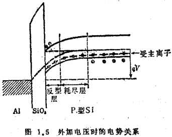
In order to discuss the working principle of a MOS field effect transistor, we assume that it has a simple structure as shown in Figure 1.4. Taking the case of N-channel as an example, when a positive voltage is applied to the gate, the potential relationship in the direction perpendicular to the silicon surface is shown in Figure 1.5. The negative charge corresponding to the positive charge induced on the gate, in addition to the negative charge such as electrons induced on the silicon surface, is also one of the acceptor ions in the space charge layer formed on the bottom surface of the P-type silicon material. Class of negative space charge. First, ignoring the influence of the space charge formed by the host ion here, it is considered that the negative charge corresponding to the positive charge induced by the gate is only the negative charge formed by the electrons induced on the silicon surface. The working principle of MOS field effect tube. When the induced carrier density is very large, that is, the gate voltage is very large, this approximation can be well established, but as the gate voltage decreases, this approximation gradually becomes invalid.
In the structure shown in Figure 1.4, the direction from the source to the drain is taken as the x axis, the length of the gate is denoted as L, and the width is denoted as W. When the source-referenced voltages VGs and VDS are applied to the gate and drain respectively, the channel potential at a point χ in the channel is denoted as N(χ). According to the reason described in the previous section, it is equivalent The gate voltage is (VGs-фMS+Vs'). The capacitance per unit area formed by the silicon dioxide film sandwiched between the conductors is denoted as C1, and the following relationship can be obtained

The leakage current at this time is recorded as IDS, and the electric field intensity in the x direction in the channel is recorded as

Eχ, then

where  it is the drift mobility of electrons in the channel, which is different from the body value of the silicon crystal and varies with the gate voltage. In the discussion in this section, let us treat the channel mobility as a constant different from the value in the crystal body. There is the following relationship between the electric field intensity in the x direction in the channel and the channel potential

So the formula (1.11) can be written as

Since IDS is the total current flowing through the channel, according to the principle of continuity of current, IDS is a constant value independent of χ, so equation (1.13) can be directly integrated, and the following equation is obtained


That is

Here, the direction of flow from the source to the drain is taken as the positive direction of the IDS. If the direction of flow from the drain to the source is taken as the positive direction, according to the meaning of the so-called leakage current, write it as ID, and the above formula becomes

This is the expression of the DC volt-ampere characteristic of the MOS field effect transistor.
In order to make the formula (1.16) hold, the N(χ) in the formula (1.10) of course cannot be zero or negative. Since V(χ) is between 0 and VDS, if

Then N (χ) no matter where it is in the channel, its value is positive, so the formula (1.16) must be established. It can be said that formula (1.17) is a necessary condition for the establishment of formula (1.16).
At this time, let us consider what happens when the formula (1.17) does not hold. First, we try to increase VDS in the area where the formula (1.17) is established, so that VGs-фMs+Vs'-VDS gradually approaches zero. At this time, the leakage current gradually approaches

It seems that there is no special performance, but when calculating the change of ID when VDS has a small change, that is, when the leakage conductance gDD is calculated, it can be obtained by formula (1.16)

We know that this formula has such a characteristic, that is, as VDS approaches (Vos-фMs+Vs'), gDD approaches zero.
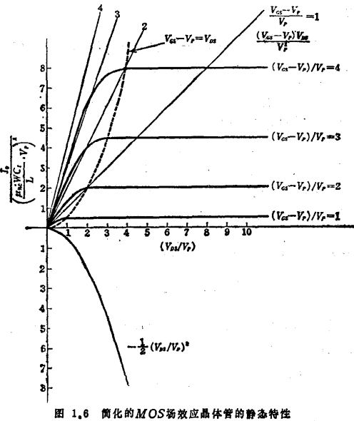
If VDS is further increased to make Vos-фMs+Vs'<VDs, then the formula (1.19) becomes gDD<0, but this area has exceeded the valid range of formula (1.16), so this conclusion is incorrect. In fact, according to the experimental results, gDD will not become negative, but will continue to take a smaller positive value. Therefore, in a rough discussion, when VGS-фMs+Vs' In the case of VDS, it can be expressed by the value when VGSфMs+Vs'=VDS. The working principle of MOS field effect tube. In other words, for gDD, in VGS-фMs+Vs'
 for VDS, take gDD=0. Based on this consideration, the volt-ampere characteristics of the entire VDS region are shown in Figure 1.6.

The VP in the figure is the voltage defined by the following formula, which is called pinch off voltage.

This is when VDS=0, such as VGS=VP, the thickness of the channel becomes zero, just like the situation when the water pipe is clamped flat.
Contact: Mr. Zou
Contact number: 0755-83888366-8022
Mobile phone: 18123972950
QQ: 2880195519
Contact Address: 5C1, Block CD, Tianji Building, Tianan Digital City, Chegongmiao, Futian District, Shenzhen
Please search WeChat official account: "KIA Semiconductor" or scan the following picture to "Follow" official WeChat official account
Please "follow" the official WeChat account: provide MOS tube technical assistance


