Electronic Technology Forum
ICM7555 time base internal circuit diagram and its function analysis
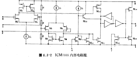
The internal circuit diagram of ICM7555 is shown in Figure 6.3-2. Corresponding to Figure 6.3-1, we can see that in the figure, M1~M4 constitute comparator 1; M5~M8 constitute comparator 2: M9~M13 and inverter constitute RS trigger; M16 is a discharge tube; M10~M15 It is a complementary output stage circuit; three 100 kiloohm resistors form a voltage divider circuit, and the divided voltage is added to the inverting input terminal of the comparator 1 and the non-inverting input terminal of the comparator 2 respectively.

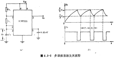
The ICM7555 time base circuit has multiple functions. It can be used not only as a monostable trigger and delay circuit, but also as a multivibrator, frequency divider, voltage-to-frequency converter, and frequency-to-voltage converter, etc. It is widely used . ICM7555 internal circuit diagram. The following introduces the multivibrator composed of ICM7555 (Figure 6.3-3a). The difference between the circuit structure of the multivibrator and the monostable trigger (Figure 6.3-1) in Figure 6.3-1a is that it is connected to the discharge loop. Timing resistor In addition, the trigger terminal 2 and the threshold terminal 6 are connected together. Once the power is turned on, the voltage Vc across the timing capacitor CT is zero. At this time, the trigger is set (S=1, R=0), and the RS trigger The output terminal Q is at a high level, and the circuit output terminal is also at a high level. In Figure 6.3-3a, the discharge tube is cut off, and the power supply voltage VDD passes through the resistor.
 and
and charge the capacitor CT so that the voltage Vc across the capacitor gradually rises, when Vc rises to
 When the output voltage of the comparator 1 changes from low level to high level, the R-S flip-flop is reset, and the output terminal voltage changes from high level to low level. ICM7555 internal circuit diagram. At this time, because the discharge tube M1 is turned on, the charge on the capacitor CT passes
 discharge, when Vc drops to
 When the output voltage of the comparator 2 changes from low level to high level, the R-S flip-flop is set again, and the voltage at the output end changes from low level to high level. In this way, the oscillation waveform of the multivibrator is obtained over and over again, as shown in Figure 6.3-3b. According to the charge and discharge equation, the pulse widths T1 and T2 can be expressed as


From the above formula, the oscillation frequency fo is

The duty cycle of the oscillating waveform is

It can be seen from the above formula that the duty cycle is always greater than 50%; in order to make the oscillation waveform close to a square wave, Should be much larger than
 。
。
Contact: Mr. Zou
Contact number: 0755-83888366-8022
Mobile phone: 18123972950
QQ: 2880195519
Contact Address: 5C1, Block CD, Tianji Building, Tianan Digital City, Chegongmiao, Futian District, Shenzhen
Please search WeChat official account: "KIA Semiconductor" or scan the following picture to "Follow" official WeChat official account
Please "follow" the official WeChat account: provide MOS tube technical assistance


