Electronic Technology Forum
Detailed analysis of the working principle of MOS field effect transistors and related devices
introduction
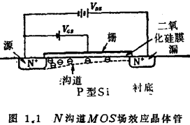
As we all know, if a voltage of appropriate polarity is applied between the metal electrode of a MOS diode and the silicon substrate, for example, when a P-type silicon substrate is used, a high positive voltage is applied to the metal electrode to make the silicon surface inverted. ). A non-rectifying electrode can be made on the inversion layer to inject carriers into the inversion layer or make the carriers flow out from the inversion layer. The device thus constituted is a MOS field effect transistor (ie MOS field effect transistor, MOSFET for short) ). If carriers are injected into the substrate from the non-rectifying electrode of the inversion layer, the amount of injection cannot be controlled by the voltage applied to the metal electrode, thus reducing the transconductance of the MOS field effect transistor, so these electrodes must be non-directional Carriers are injected into the substrate. As shown in Figure 1.1, there is a barrier corresponding to the diffusion potential at the electrode that uses the P-N junction to inject carriers to prevent the injection of carriers into the substrate.
It is equivalent to the inversion layer part of a MOS diode, as shown in Figure 1.1. As will be mentioned below, carriers flow along the silicon surface, which is called a channel in the sense of a current path. The electrode that injects carriers into the channel is the source of the carriers, so it is called the source, and the electrode that flows out of the carriers from the channel is the outlet of the carriers, in this sense it is called the drain ( drain). In principle, the source and drain are non-rectifying electrodes for the channel, so they are equal. In fact, sometimes the two cannot be distinguished. In the structure of the ring gate, the electrode on the inner side of the gate is used as the drain. When using an N-type inversion layer, a voltage should be applied between the source and the drain according to the polarity shown in Figure 1.1. At this time, the positive voltage must be increased to the metal electrode of the MOS diode. On the contrary, if the negative voltage is increased, the N-type inversion layer will disappear, and no current will flow between the source and the drain. The working principle of MOS field effect transistor. In other words, the current flow between the source and the drain is controlled according to the voltage applied to the metal electrode. This electrode functions as a "valve" that controls the channel current, and is called a gate in this sense.

It is generally believed that as long as the surface of the substrate is oxidized, a selective diffusion is performed at the place equivalent to the source and the drain, and the gate metal is evaporated, the MOS field effect transistor is generally manufactured. Therefore, compared with the junction transistor, it seems that there are fewer processes. And easy to manufacture. But in fact, the nature of the silicon dioxide film, the interface state density between the silicon dioxide film and the silicon ● and its properties, and the form of the scattering of carriers flowing along the interface, are sensitive to changes with the process, and cannot be changed due to the process. Assert that less is easier to make.
When a large positive or negative gate voltage is applied to the substrate, the situation at the interface between the silicon and silicon dioxide film is generally clear. Now let us look at the situation where the gate voltage is zero. Because the work functions of metal and silicon are not necessarily equal, even if the gate voltage is zero, as shown in Figure 1.2 (a), the surface potential is never zero. The working principle of MOS field effect transistor. In order to make the MOS diode in a state where the surface potential is zero, that is, to realize the so-called "flat band con-dition", a voltage of фMS=(фM-фS) relative to the substrate needs to be applied to the gate electrode, such as As shown in Figure 1.2(b). Here фM and фS are the electrostatic potentials corresponding to the work functions of metal and silicon, respectively. When there is a work function difference us between metal and silicon, the flat-band condition can be realized by adding the voltage of -фMS according to a simple theory without deliberately adding the gate voltage from the outside.

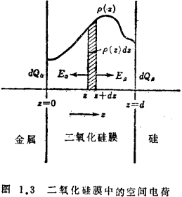
Another reason why the silicon surface potential is not zero when the gate voltage is zero is that the Na+, Si+, and O- plasma contained in the silicon dioxide film constitute space charges. Let's study specifically, when the space charge distribution in the silicon dioxide film is given, what kind of effect will it have on the potential of the silicon surface. The working principle of MOS field effect transistor. As shown in Figure 1.3, suppose the space charge density p(z) in the silicon dioxide film is known, and take the origin z=0 as the interface between silicon dioxide and the metal electrode, and take the z-axis perpendicular to the silicon surface. The interface between the silicon oxide film and silicon is at z=d.

When there is a space charge p(z)dz in the tiny area of z and z+dz, the electric field intensity generated between this space charge and the metal electrode is denoted as Eo, and the electric field intensity generated between the space charge and the silicon is denoted as EB. Because of the action of these two electric fields, the charge density induced on the metal electrode and silicon surface is dQo and dQβ respectively. ε1, taken as the dielectric constant of silicon dioxide, obtained from Gauss's law

and

relationship. Because it is considered that the gate voltage is at zero, the potential of the metal and the silicon substrate are equal, then

Must be established. Solve equations (1.1) and (1.4) simultaneously to solve Eo and Eβ, and then substitute the obtained values of Eo and Eβ into equations (1.2) and (1.3), we get

From formula (1.6), the total charge density QB induced on the silicon surface can be obtained as

To achieve flat band conditions, a voltage must be applied to the gate to make the charge density induced on the silicon surface disappear. This voltage is recorded as Vs', because the flat band condition is established when Vs' is applied, and there is no voltage drop in silicon, so all external voltages are applied to both ends of the silicon dioxide film. The working principle of MOS field effect transistor. Therefore, if the electrostatic capacitance per unit area of the silicon dioxide film sandwiched between the metal electrode and the silicon substrate is denoted as CI, that is

Then there is

In other words, in order to achieve the flat band condition, the gate needs to be applied with a voltage Vs' relative to the silicon substrate. Therefore, when there is space charge in the silicon dioxide film, in order to realize the flat band condition, according to a simple theory, the effective gate voltage Vs' is applied to the gate.
Contact: Mr. Zou
Contact number: 0755-83888366-8022
Mobile phone: 18123972950
QQ: 2880195519
Contact Address: 5C1, Block CD, Tianji Building, Tianan Digital City, Chegongmiao, Futian District, Shenzhen
Please search WeChat official account: "KIA Semiconductor" or scan the following picture to "Follow" official WeChat official account
Please "follow" the official WeChat account: provide MOS tube technical assistance


