Electronic Technology Forum
Analysis when there are space charges formed by impurity ions in the MOS field effect crystal substrate
The previous section ignored the space charge formed by impurity ions in the substrate 2), and we take it into consideration in this section. In order to obtain the volt-ampere characteristics of a MOS field effect transistor, you can try to find the voltage distribution at each point when a voltage is applied between the gate source and the drain source and the corresponding charge distribution.
The direction from the source to the drain is taken as the x-axis. For example, the applied voltage across the silicon dioxide film at a certain point in the channel is recorded as Vo(χ), as shown in Figure 1.7

Where
ψs is the silicon surface potential source end of the semiconductor body when used as a reference. The value of ψs is a function of the gate voltage, written as ψso (VGs), and the channel potential V (χ) is defined by the following formula:

The formula (1.21) can be written as

If the surface charge density of electrons in the channel is denoted as QB, the space charge density QB formed by holes and acceptors in silicon is


Where
p is the hole density, n is the electron density,![]() is the acceptor density.
is the acceptor density.
If the positive charge density on the metal electrode is recorded as QM, then

According to Gauss's theorem, obviously there are the following relations

If the channel width is denoted as w, the drain-source current IDS is

Such as substituting the following two formulas

then

On the other hand, from equation (1.26) we know

Because QB is also related to voltage, let's find QB3 below).
From the formula (1.24)

where

ψp is the electrostatic potential in the P-type semiconductor body
ψF is the Fermi potential calculated from the center of the band gap, that is, the difference between the electrostatic potential and the Fermi potential assumes that the quasi-Fermi level of the hole is consistent with the value of the thermal equilibrium Fermi level.
F(U, ξ, UF) is a quantity defined by the one-dimensional Poisson equation, as shown in the following formula.

where , Ψn is the quasi-Fermi level of electrons.
Obviously, at the source end, the quasi-Fermi level of the electron is equal to the quasi-Fermi level of the hole and the Fermi level in the semiconductor body, so it can be understood as

(Where ψnψp is the quasi-Fermi potential of conducting electrons and holes calculated from the center of the band gap, respectively). At this time, formula (1.33) can be directly integrated to obtain

The following is divided into three areas according to the Z axis, respectively, try to find the approximate value of F (U, ξ, Up). However, these three regions do not necessarily correspond to the inversion layer, the depletion layer, and the P-type region.
(1) Area

Then there is

(2) Area

which is

Then there is

(3) Area

which is

Then there is

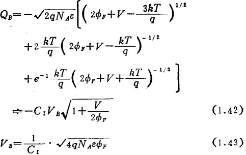
QB is the sum of the results of substituting formula (1.37), (1.39), (1.41) into formula (1.32)

Substituting formula (1.42) into formula (1.31), and substituting the result into formula (1.30) to solve, we get

Equation (1.44) is the expression of the DC volt-ampere characteristics of the MOS field effect transistor. With this formula, as in the previous section, several important parameters can be derived.
First calculate the leakage conductance. As in the previous section, take the current flowing into the leakage as the positive direction of the leakage current, and get

According to the definition in the previous section, the gate voltage of gDD=0 when VDs=0 is called the pinch-off voltage VF, then

Use this formula to express the leakage conductance, then

Leakage current can be written as

If formula (1.48) is used, at that time, the leakage conductance becomes zero. Regarding the subsequent state, the same as the previous section, even if the drain voltage increases. It can still be regarded as a state where the continuous leakage current is zero. This is also an approximation.

Contact: Mr. Zou
Contact number: 0755-83888366-8022
Mobile phone: 18123972950
QQ: 2880195519
Contact Address: 5C1, Block CD, Tianji Building, Tianan Digital City, Chegongmiao, Futian District, Shenzhen
Please search WeChat official account: "KIA Semiconductor" or scan the following picture to "Follow" official WeChat official account
Please "follow" the official WeChat account: provide MOS tube technical assistance


