Electronic Technology Forum
MOS field effect transistor frequency conversion (mixing) circuit principle work and example analysis
This circuit is also the same as the high-frequency amplifier circuit. Its advantage is that it can reduce the mixing of clutter signals by using the square-law characteristics. If it is a complex gate type, there is less useless radiation. At present, it is mostly used in advanced FM receivers.
●)The crystal oscillator can only excite odd oscillations.

In order to give full play to the characteristics of field effect transistors, a separately excited circuit that works stably and may make the local oscillator level and mixing effect the best should be used. The following only describes this aspect.
(1) The work of the frequency conversion circuit
The ability of the frequency conversion circuit can be expressed by the conversion gain, namely

At this time, the definition of various gains similar to (amplified) power gain can be obtained. Gc
Can be expressed as

Where Is the input conductance of the field effect transistor at the signal frequency,
 Is the output conductance of the intermediate frequency, g2● is the loss conductance of the output coupling circuit, gL is the load conductance, and gL is the variable frequency conductance, which can be written as

●)But there is also a source injection method.
it is the intermediate frequency output current when the output terminal is short-circuited.Where is the signal voltage at the input,
(2) Variable frequency conductance of single-gate MOS field effect transistor 37)
For the mixing operation of single-gate MOS field effect transistors, the injection position of the local oscillator power is considered to be the insulated gate G1, the base gate G2, and the source. Although the injection into G2 is also effective, the base of the MOS field effect transistor is usually connected with the tube base, which may generate local oscillator radiation, so it is not suitable to use 38). When injected from a source, since the source cannot be grounded at high frequency, there is the disadvantage of reducing the gain ●). So, let's talk about how the local oscillator and signal are added to G1.
Suppose VL is the peak voltage of the local oscillator. When a small signal approximation is used, the variable frequency conductance gc can be written as

When gm has the square law characteristic of formula (2.5), gc can be written as

As long as the peak value of the local oscillator voltage + signal voltage is lower than VGS-VT, the above equation holds true even if it is not a small signal. When increasing the local oscillator voltage for positive excitation, before Id will reach saturation, gc is at its maximum value, increasing to 0.38gmmax. gmmax is the maximum value of gm under positive excitation. However, in order to take full advantage of the field-effect transistor, its operating point should be limited to the square-law characteristic area ●). In FM receivers that use field-effect transistors to form the mixing stage, there are actually some poor cross-talk modulation characteristics due to excessive local oscillator voltage 39).
●) For this reason, the voltage applied to the gate requires that its negative peak value does not stop the ID, and its positive peak value does not make the working area of the field effect transistor reach the shoulder of the triode area.
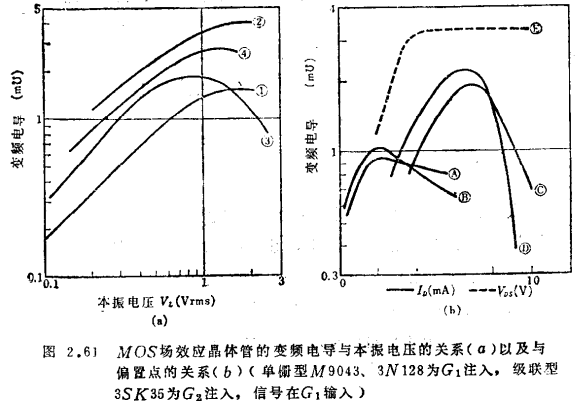
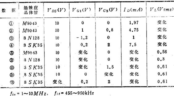
The curves ①②③and  in Figure 2.61 show the relationship between the variable-frequency conductance gc of a single-gate MOS field effect transistor and the local oscillator voltage and bias current. The figure also shows that the size of gc can be adjusted by the substrate bias.


(3) Variable frequency conductance of cascaded MOS field effect transistor
Of course, the cascaded MOS field effect transistor can also be used as a single-input device to produce frequency mixing, but in order to take advantage of the characteristics of this cascaded type, it is best to apply the local oscillator voltage and signal voltage to different gates. . Taking into account the stability of the intermediate frequency and the local oscillator radiation, the local oscillator voltage is usually added to G2, and the signal voltage is added to G1.). At this time gc can be expressed as (small signal approximation)

The gc of the cascaded MOS field effect transistor changes slightly with bias conditions 40). The curve ④ and  in Figure 2.61 show the relationship between gc and the local oscillator voltage and offset. Because of the large change with ID, attention should be paid when adjusting.
The cascaded G2 has a low voltage feedback to G1, about 0.1. Taking into account the problem of clutter radiation, it is more advantageous to adopt the G2 injection method.
(4) Frequency conversion circuit ●●) 41)
The input and output ends of the frequency conversion circuit are usually conjugate matched at the respective signal frequency and intermediate frequency. When the signal frequency and the intermediate frequency are far apart, the input circuit can be short-circuited to the intermediate frequency and the output circuit to the signal frequency, and the frequency conversion stage is not easy to cause oscillation. But in order to make the secondary (intermediate frequency stage) stable, the output conductance of the variable frequency stage is often used as the mismatched load of the secondary input.
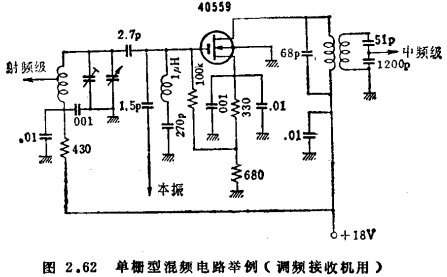
When the signal and the local oscillator are applied to the same electrode, the local oscillator is added through a small capacitor or through a small ring coupled with the input coil. When the input coil and the grid are coupled through a small capacitor, the intermediate frequency series resonant circuit must be connected to the grid to make it short-circuit to ground at this frequency. Figure 2.62 is an example of this kind of frequency conversion circuit using a single-grid tube, which is designed for an FM receiver. At this time, the load that is overlooked is designed to be 8kΩ (including g2●). The substrate base of 40559 has a voltage of 3V to the source, G1 is biased at 1V, I①=3mA, in addition, the local oscillator voltage is
 . Under this condition, when the frequency conversion operation of 100MHz→10.7MHz is performed, the parameters are
 ,
, ,
, therefore, if the conversion gain of this stage is calculated according to formula (2.124), excluding the loss caused by g2● (the gain of the load from G1 to D), it can be 21.3dB.
●)Of course, there is also a method of adding local oscillator and signal voltage to G1 at the same time, and there is also a method of adding local oscillator voltage to G1 and signal voltage to G2.
An example of the cascade type for the same purpose is shown in Figure 2.45. The gate bias of 40604 is
 ,
, ,in
,in when the local oscillator voltage applied to G2 is
 . In this case, there are
 ,
, ,
,

. When the output is matched, the conversion gain is 23.2dB. If there is a mismatch loss, the conversion gain is 18dB.
The single gate type source injection circuit, the cascade type G1 injects the local oscillator signal and G2 adds the signal circuit are shown in Figure 2.63 and 2.64, respectively.

Contact: Mr. Zou
Contact number: 0755-83888366-8022
Mobile phone: 18123972950
QQ: 2880195519
Contact Address: 5C1, Block CD, Tianji Building, Tianan Digital City, Chegongmiao, Futian District, Shenzhen
Please search WeChat official account: "KIA Semiconductor" or scan the following picture to "Follow" official WeChat official account
Please "follow" the official WeChat account: provide MOS tube technical assistance


