Electronic Technology Forum
Examples of CR Coupling and Distributed Amplifiers of MOS Field Effect Transistor Broadband Amplifier
Broadband amplifiers are also useful for tuning amplifiers (such as staggered tuning, etc.), here only the CR coupling and the method of using distributed amplifiers are described.
(1) CR coupling amplifier
From the equivalent circuit of a unit (from the gate to the secondary gate) of the CR-coupled multi-stage amplifier shown in Figure 2.65 (b in the same figure), it can be seen that the frequency at which the voltage gain is 3dB lower than the intermediate frequency domain is

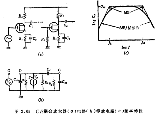

The gain of each frequency domain is

Source bypass capacitor in the picture Should be chosen greater than
 ;among them
 。This gives the gain-bandwidth product
 for
for

For the high-frequency MOS field-effect transistors shown in Table 2.1, this value is about 200MHz or less and only the gains in the mid-frequency domain and the high-frequency domain are considered. MOS field effect transistor broadband amplifier. When the amplifier with this characteristic is cascaded by n stages, a 3dB upper limit frequency will press

cut back. Therefore, even if the required bandwidth is lower than , Increasing the number of stages may not be able to meet the requirements of gain-bandwidth at the same time.
 can also write

This formula differentiates n and makes the derivative equal to 0, so given from time to time
 the maximum value of n is

In addition, the gain of the first stage for
for

 At a certain time, when the number of stages is
 maximum. For example, if a device with a GB product of 200MHz is used to make the bandwidth(
 )Is a 60MHz amplifier, from the following formula

It can be seen that there is at most 8 levels, at this time It is limited to a maximum value of 34.7dB. It can be seen that the efficiency of this amplifier is not high.
For this reason, measures must be taken on the inter-stage circuit to try to expand the frequency band. The theory proves that when a four-terminal network is used in the inter-stage circuit (see Figure 2.66 (a), no matter how complicated it is), the GB product can be improved by 3.94 times at most; MOS field effect transistor broadband amplifier. When using both ends of the network ((b) in the same figure), the improvement can be doubled at most.
In fact, a relatively simple circuit as shown in Figure 2.67 (parallel peak building circuit) is used. At this time, the voltage gain is

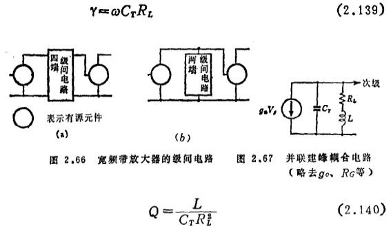
One of the selection criteria of this circuit constant is to try to obtain the maximum flatness of the amplitude, that is, the absolute value of the gain is as high as possible in  and the high-order derivative value is taken as 0.
In this way, the phase characteristics can be better maintained, and the pulse characteristics can also be better maintained. This characteristic can be obtained when Q=0.415, and the -3dB upper limit frequency is 1.72·(2πRLCT)-1. In other words, the degree of improvement is 1.72 times.
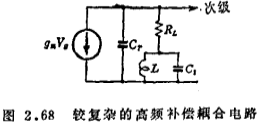
For a slightly more complicated circuit, such as Figure 2.68, the conditions for obtaining the maximum flat characteristic are
 , The upper limit frequency improvement degree is 1.85 times.
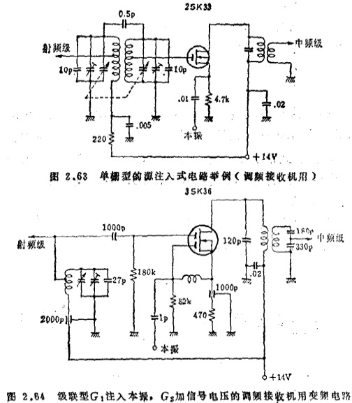
Practical circuits for MOS field effect transistor video amplifiers include preamplifiers for light-guided camera tubes 43) 44). At this time, in order to obtain an excellent S/N ratio, it is required

Value is greater. High frequency MOS field effect transistors are more suitable, but due to the large 1/f noise, they are not as good as junction field effect transistors. 43) 44)
(2) Distribution amplifier
The distributed amplifier is formed by adding several active components in parallel on two input and output lossless delay lines with respective characteristic impedances at both ends, as shown in Figure 2.69. MOS field effect transistor broadband amplifier. Let L and C be the parameter values of the unit length of the delay line, then the phase velocity in the LC delay line
 available
 Indicates that in order to synchronize the waves on the gate delay line and the drain delay structure, the following formula must be established
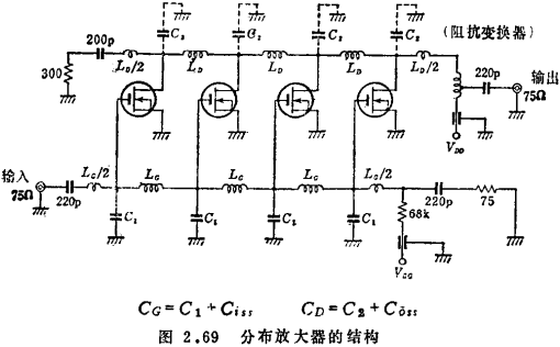

CD and CG contain the input and output capacitances of MOS field effect transistors. Suppose the series resistance of L is R and the parallel conductance of C is G, then the characteristic impedance Zo of this delay line is

When R and G are 0, Zo is equal to . R can usually be ignored, but G sometimes cannot be ignored. At this time, the delay line cannot be terminated with pure resistance, because signal reflection will deteriorate the frequency band characteristics, and special measures should be taken to compensate ●). From this point, it can be said that MOS field effect transistors (similar to vacuum pentodes) with high input and output impedance are suitable for distributed amplifiers. However, the cut-off frequency of the delay line approximated by a lumped parameter system like Fig. 2.69 is
●)例如,使各L间有一定互感。

At frequencies higher than fc, the gain will change. At frequencies below fc, the voltage gain and power gain of the system can be obtained by the following two equations respectively

As an example of a distributed amplifier using MOS field effect transistors, there is an amplifier applied to cable television 45). In this example, 4 field-effect transistors of model MEM557 are used. ,
, , Including stray capacitance
 About 5.0pF,
 When used under the condition of about 3.5pF), a power gain of 11dB can be obtained (Figure 2.69).
by ,
, can be found
 and
and
 the value of the component can be obtained by setting the leakage additional capacitance to 0
 and
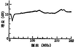
and value. In order to take out the output signal with the coaxial cable, a variable transformer for impedance conversion must be used. MOS field effect transistor broadband amplifier. The gain deviation of the completed amplifier is shown in Figure 2.70, and the cross-talk modulation characteristics are also very good. This amplifier can be used in practice.
Contact: Mr. Zou
Contact number: 0755-83888366-8022
Mobile phone: 18123972950
QQ: 2880195519
Contact Address: 5C1, Block CD, Tianji Building, Tianan Digital City, Chegongmiao, Futian District, Shenzhen
Please search WeChat official account: "KIA Semiconductor" or scan the following picture to "Follow" official WeChat official account
Please "follow" the official WeChat account: provide MOS tube technical assistance


