Electronic Technology Forum
Overview of MOS Field Effect Transistor Weak Current Amplifying Circuits and Measuring Methods
There are three types of circuit structures usually used to measure weak currents as shown in Figure 2.86. In the circuit of Figure 2.86(a), the signal current is can be Find. Due to the effect of negative feedback, the input impedance is reduced to
 (G is the voltage gain of the amplifier), so it is suitable for measuring the current when the signal source terminal is short-circuited. In contrast, the input impedance of the circuit in Figure 2.86(b) is increased to
 ,It is suitable for measuring the open circuit voltage of the signal source terminal. MOS field effect transistor weak current amplifier circuit. Figure (c) uses an integrator to integrate the signal current. The signal current is calculated according to the growth rate of the integrated voltage. Its characteristic is that the induced noise of the mains power frequency is averaged and removed.

The sensitivity of these methods are all restricted by the drift of the amplifier circuit. Drift can be equivalently divided into the leakage current id (current source) and voltage drift vd at the input end of the amplifier shown in Figure (a). The output voltage is

Where

Signal-to-noise ratio 。
。
Radiation detectors, photoelectric tubes, etc., where the internal resistance can be roughly regarded as infinite, because Zf can be very large, and the υd term can be ignored compared with id, so a small id amplifying element is specially used. PH (pH) meters, biological potential detectors and the like are different, and their internal resistance is below a moderate level (below tens to hundreds of MΩ), id and vd should be considered 52) 58).
The id of the MOS field effect transistor is the variable component of the gate current 54). The gate current is ultimately restricted by the leakage current of the silicon dioxide film, and high sensitivity below 10-16A is expected. In fact, compared with the leakage current of the silicon dioxide film, the leakage current component at the sealing of the case and tube is dominant. MOS field effect transistor weak current amplifier circuit. As shown in Figure 2.87, the gate current Ig is a combination of the drain and source components IgL1 and IgL2 flowing into the grid through the sealing glass, and the components Is1 and Is2 flowing into the grid through silicon dioxide, and can be expressed as

IgL1 and IgL2 are mainly determined by the surface pollution of the sealing glass and the absorption current of the glass medium. For devices that have been placed indoors for a long time, the gate current generated by surface contamination can reach about image.png, which can be restored to about 10-15A after being cleaned with ethanol and dried. In order to stabilize the sensitivity of about 10-15A for a long time, it is necessary to adopt a structure with a lead spacing of more than a few mm for package packaging (the sealing material is glass or surface-treated frozen stone, etc.), and at the same time, the start-up caused by the absorption of the medium Time drift is also significantly reduced. The devices packaged in such a sealed package are not yet commercially available, but as shown in Figure 2.88, it is better to solder the devices cleaned by ethanol to a suitable package for packaging. At this time, the inside of the shell does not need to be evacuated. When using cast plastic resin for encapsulation, impulse noise is generated due to the internal stress of the resin to form polarized charges, and it takes a long time for this noise to disappear.
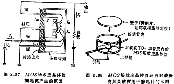
Figure 2.89 is an example of measuring the gate current. (I) It is a pipe with a dirty surface. The leakage resistance is about 2×10¹⁴Ω. (ii) is a general qualified product. If the lead spacing is widened, as shown in (iii), the leakage resistance can be improved to 2×10¹⁶Ω. Figure 2.90 is an example of measuring the absorbed current of the usual TO-18 type shell sealing glass, which can reach a stable state in about 3 minutes.
The magnitude of the drift current caused by the voltage drift υd can be obtained by formula (2.154)

Where

The size of υd is related to the DC operating point. If the operating point is properly specified, υd can be below a few +μV/℃; recently, pairs of tubes with consistent characteristics are used to form a differential amplifier circuit, and 100~200μV/℃ can be obtained without adjusting the operating point. Υd.
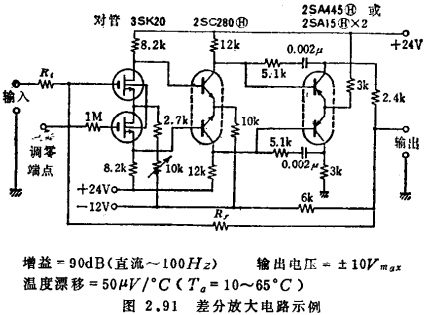
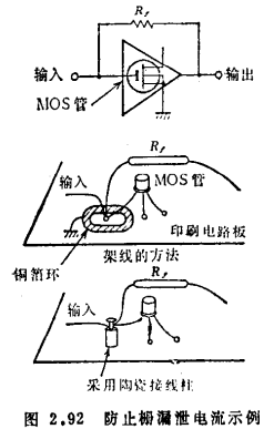
Figure 2.91 is an example of a typical differential amplifier circuit. Using Rf=1016~1012Ω, the current sensitivity of about 1×10-15A can be obtained. Suppose the voltage drift is 100μV/℃, and Rf=1×10-15A/℃. The second or third stage circuit adopts a bipolar transistor differential amplifier circuit with a stable DC operating point. MOS field effect transistor weak current amplifier circuit. In the circuit structure, it should be noted that the gate of the primary field-effect transistor should be connected to the input terminal through a highly insulating frozen stone or PTFE joint. This is to prevent leakage current from the nearby amplifier power wiring via the surface resistance of the printed circuit board (see Figure 2.92).
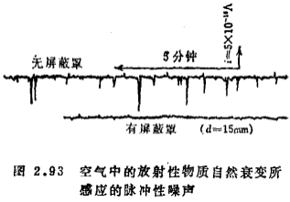
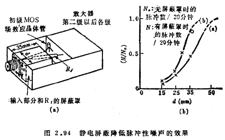
Attention should be paid to the wiring to avoid damage to the gate insulating layer when soldering or unintentionally touching the gate electrode by hand. Since the gate input capacitance is about 3pF, for the mains frequency of 50 or 60Hz, the gate impedance is about 1000MΩ. Therefore, if the leakage resistance of the soldering iron is below this level, a voltage of about 100V will be applied to the grid during wire bonding. For this reason, the grid and other electrodes (source or drain) should be short-circuited or the road iron should be grounded in advance. In addition, the human body is particularly susceptible to electrification in winter. If you accidentally touch the open gate electrode with your hands, it will generate an example voltage of more than 200V to prevent the leakage current of the shed, which often causes the gate to be destroyed in an instant. As long as the grid is short-circuited during the wiring operation, the above situation can be prevented. For the weak current amplifier circuit, because the negative feedback resistance, input resistance and other values are very large, it is easy to produce various electrostatic induction. MOS field effect transistor weak current amplifier circuit. Therefore, electrostatic shielding of the input circuit is essential. Electrostatic shielding can also attenuate the impulse noise induced by the natural decay of natural radioactive substances in the air (mainly radon (Rn)) 55).
The alpha particles produced by the natural decay of radon collide with air molecules to cause primary ionization and secondary ionization, which can produce ion pairs of about 10-14 Coulombs. When this kind of ion pair moves along the electric field near the amplifier input circuit, its electrostatic induction current forms impulsive noise. Because the electrostatic shielding can cut off the a particles from the outside and reduce the amount of internal air at the same time, it has the effect of reducing the frequency of natural attenuation. Figure 2.93 is an example of this impulsive noise.
As shown in Figure 2.94(a), when the gate lead of the MOS transistor and the negative feedback resistor Rf are used for electrostatic shielding, the relationship between the shielding cover volume and the number of pulses is shown in Figure 2.94(b).
From the formula (2.154), the gain (conversion impedance) of the weak current amplifier circuit can be written as

Therefore, the DC gain is the negative feedback resistance Rf, but because Rf is high resistance, a little stray capacitance Cf connected in parallel with Rf restricts the entire bandwidth. For example, if Rf=1×10¹²Ω, Cf=0.1pF, the bandwidth (-3dB) is

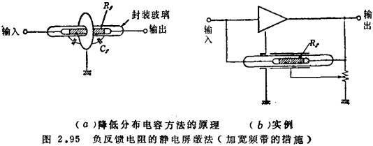
Generally speaking, it is much lower than the bandwidth of the amplifier's open loop gain G. For this reason, to widen the frequency band, first try to reduce Cf.
Figure 2.95(a) is an example. The negative feedback resistance Rf passes through the electrostatic shielding plate support, and grounds Cf to reduce the negative feedback capacitance; Figure 2.95 (b) is an improved method, Rf is added to the shielding cover, and the conductive metal tube is wrapped at the same time to try to reduce Rf capacitance to ground. When such measures are taken, the above-mentioned bandwidth can be improved by about one or two orders of magnitude.
Contact: Mr. Zou
Contact number: 0755-83888366-8022
Mobile phone: 18123972950
QQ: 2880195519
Contact Address: 5C1, Block CD, Tianji Building, Tianan Digital City, Chegongmiao, Futian District, Shenzhen
Please search WeChat official account: "KIA Semiconductor" or scan the following picture to "Follow" official WeChat official account
Please "follow" the official WeChat account: provide MOS tube technical assistance


