Electronic Technology Forum
MOS field effect transistor high frequency (RF) amplifier circuit characteristics, signal, control, design details
The function of the high-frequency amplifier circuit in the receiving system is (1) improving the signal-to-noise ratio, (2) reducing the received clutter signal, and (3) preventing unwanted radiation such as local oscillation. To this end, there should be (1) low-noise and high-gain amplifying components, (2) good pre-selection circuits and amplifying components with low nonlinearity, and (3) shielding of the emission source, etc., and consideration should be given to the high-frequency level Measures such as buffering and notching.
In addition, when the high-frequency stage uses the bias characteristic of the amplifier element to perform automatic gain control, it is necessary to be able to fully control the gain, and it is required that the frequency band characteristics at this time are not distorted.
The advantage of using MOS field effect transistors as high-frequency amplifier elements is that the transfer characteristics are square-law characteristics, and the double-signal distortion such as crosstalk modulation caused by the nonlinearity of the third or higher harmonics is small, so the influence of clutter signals is small, and Due to low input conductance, selectivity can be improved. MOS field effect transistor high frequency (RF) amplifier circuit. Especially the cascaded gate type MOS field effect transistor, because the feedback capacitance is small, the work is stable, the frequency deviation during automatic gain control is also small, and because the gain control electrode can be separated from the input, the crosstalk modulation characteristics are also particularly good. Started to be used in the high frequency part of VHF TV. FM broadcast receivers are also used simultaneously with junction field effect transistors.
(1) Noise characteristics
The noise figure Fo of the entire receiving system can be expressed as follows:

In order to reduce Fb, F1 should be reduced, and G1 should be increased so that the influence of F2 is negligible (about 10dB or more).
The relationship between the noise figure, gain and bias point of MOS field effect transistors is shown in Figure 2.33. The relationship between noise figure and signal source admittance is shown in Figure 2.34.
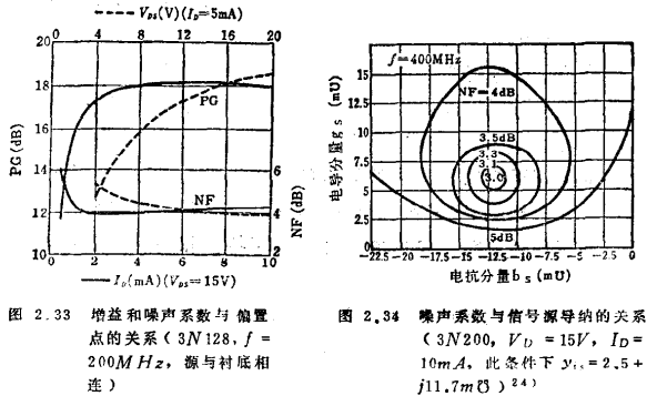
It can be seen from the figure that the best points of noise characteristics and amplification characteristics are generally inconsistent, and a compromise value between the two should be used.
Put the tuning loop, etc. in the circuit before the preamplifier element, and its circuit insertion loss directly causes the deterioration of the noise figure, so the QL/QL of the tuning loop should be small.
(2) Automatic gain control
Although there is also a method using dedicated attenuation elements, it is also possible to change the bias current ID and bias voltage VDs of the amplifying element to achieve automatic gain control. This method is more economical.
When adding automatic gain control, it is hoped that the frequency characteristics and dynamic range of the amplifier will not change.
For example, the input admittance yin of the amplifying element can be written as

When the source is grounded, at the intermediate frequency, ,
, ; When tuning, yo+yL→go+gL, so yin is

The third term is the increase in input capacitance caused by feedback, which is called the Miller effect. Therefore, if the CTS is large, the tuning frequency will shift in the automatic gain control. In addition, when adding neutralization and preventing this phenomenon, it is also affected by the change of the CTS with the bias voltage. MOS field effect transistor high frequency (RF) amplifier circuit. In addition, if the CTS is very large, the resulting signal leakage will make the automatic gain control variable range not wide enough.
For the automatic gain control of single-gate MOS field effect transistors, there are methods of changing the gate bias to reduce ID (reverse automatic gain control) and methods of reducing VDs. When the latter method is adopted, it is generally connected in series or parallel with other variable impedance components (quasi-positive automatic gain control).
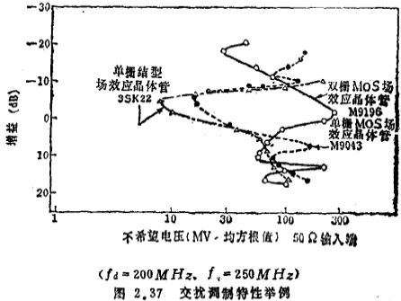
For reverse automatic gain control, the substrate grid can also be used for automatic gain control, but because the control sensitivity is not high, this method is mostly not used. Generally, a signal and automatic gain control voltage are added to the insulated gate. The CTS of this method is about 0.13PF, and the automatic gain control range is about 30dB when neutralization is not added at 200MHz, and about 50dB when neutralization is added. Single-gate field effect transistors are sharp cut-off transistors, and the crosstalk modulation characteristics or large signal characteristics will deteriorate at high attenuation (see Figure 2.37. In the end, the signal path is only related to CTS and can be improved again).
For the positive automatic gain control, the degradation of the crosstalk modulation characteristics is relatively light, but at low VDs, the CTS increases, which makes the range of the automatic gain control smaller (20dB is weak when the neutralization is not added at 200MHz. The neutralization is 30dB).
If it is a cascade type (including multiple gate type), the automatic gain control voltage is generally applied to the rear stage (second gate G2), and 60dB control can be obtained at 200MHz, but it can also be applied to the first gate at the same time. In other words, if the reverse direction is applied to G2 and the forward automatic gain control voltage is applied to G1, or a fixed forward bias is applied to G1, the crosstalk modulation characteristics can be improved. However, in the former case, due to the increase of CTS, The automatic gain control range is limited to about 35dB. MOS field effect transistor high frequency (RF) amplifier circuit. If the reverse automatic gain control voltage is added to G1 at the same time, the control sensitivity will increase, because the field effect transistors of the front and rear stages all work in the pentode area. The input capacitance is reduced, so the frequency change is also small. (3)
CTS must be reduced to reduce the center frequency offset of automatic gain control. Especially difficult to do above 100MHz
To completely neutralize, so it is important to reduce CTS. It can be seen from the example in Figure 2.35 that the single-gate type cannot be used in the RF stage for VHF TVs, while the cascaded-gate type has begun to enter the practical stage.
(3) Clutter signal connection
The special clutter signal connection in the superheterodyne receiver is related to the input interference signal fin with the following relationship: When n. M takes a positive integer, ▏n Ⅹinput signal frequency fin±mⅩlocal fL▕=IF
Especially when m=n=1,

It becomes 1/2 IF interference. This interference can be reduced if the selectivity of the radio frequency part is maintained and the use of non-linear components in the radio frequency stage and the mixing stage can be reduced. The MOS field effect transistor has high input impedance, and its selectivity can be improved by a simple circuit. In addition, it is also good from a linear perspective.
Two-signal interference includes cross-talk modulation and mutual modulation.
When both the useful signal and the interference signal enter the receiving system, due to the non-linearity of the components, there will be a cross-talk modulation phenomenon in which the useful signal changes with the size of the interference signal. Therefore, when the interference signal has amplitude modulation, even if the useful signal is not modulated, the output signal is equivalent to being modulated. If the modulation degree of the interference signal is mu and the signal amplitude is υu (root mean square value), then the modulation degree (cross-talk modulation degree) m of the output signal is

In the formula, gm″ is the second-order differential of gm to the input voltage, and K is called the cross-talk modulation index ●). Generally, the υu value when K=1% represents the cross-talk modulation characteristics.
Intermodulation is the response obtained when the sum or the difference of the integer multiple of the two frequencies is consistent with the receiving frequency, and its magnitude is also closely related to the crosstalk modulation characteristics. In order to improve the characteristics of cross-talk modulation and inter-modulation, while selecting components with low non-linearity, the selectivity of the pre-tuning circuit should be improved, the amplification should be suppressed so that the latter stage should not be saturated, and the antenna input voltage should not be increased as much as possible. , Lead it to the primary amplifying element. For this kind of distortion, because there is no remedy for the later stage, special attention should be paid to the beginner.
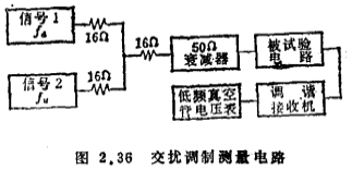
When measuring the crosstalk modulation characteristics of the amplifying element, in order to facilitate the measurement, the circuit composition of Figure 2.36 can be used, and it is more convenient to measure in the form of input non-tuned and output tuned circuits ●). Sometimes automatic gain control is often added to the radio frequency stage, so it is necessary to use a method that represents the relationship between the attenuation and υu at the maximum amplification amount. This characteristic has various differences due to the different amplifying components used and the method of adding automatic gain control bias 14).
●)It can be seen from formula (2.104) that when the transfer characteristic is an ideal square-law characteristic, gm''=0, no cross-talk modulation occurs. In addition, when the useful signal and the interference signal are FM signals, the input tuning circuit undergoes slope discrimination and receives amplitude modulation, causing interference, and may also be accompanied by phase changes, so crosstalk modulation becomes a problem when the interference signal is large.
Figure 2.37 is an example of measurement of crosstalk modulation characteristics, which exhibits complex changes as the offset changes. For example, from the gm~VG1 characteristic curve in Figure 2.11, it can be seen that υu decreases when passing through a position with a large curvature ●).
(4) Examples of high-frequency amplifier circuit design 15)~20)
Listed below is the design of a high-frequency amplifier circuit for an FM receiver using a single-gate MOS field effect transistor 3N128. First, try to design a non-neutralized circuit with input and output tuning.
If a variable capacitor of 6~18pF is used to cover the tuning of 75~91MHz, there must be an inductance of 0.12μH and an additional capacitance of 19.8pF. MOS field effect transistor high frequency (RF) amplifier circuit. The selectivity requires that the attenuation of the mirror frequency is above 45dB. Set the QL of the input and output tuning loops to be 30 and 40 (set center frequency 76MHz, intermediate frequency 10.7MHz), and their respective attenuation degrees are 22.7 and 26dB respectively, a total of 48.7 dB. If designing at 90MHz, take the bias point of 3N128 as VDS=15V, ID=5mA, then the y parameter is

●)In this way, the crosstalk modulation characteristics of the component itself can be measured.
●)In other words, at the position of O (inflection point) in Figure 2.11, the slope of gm to VG1 is the largest, but the third-order distortion is the lowest. In addition, the ● point is the place where the second-order distortion is the lowest, but the third-order distortion is the largest. It is hoped that the bias should be close to the O point during low crosstalk modulation, and the bias should be close to the ● point when the mixing effect is maximized.
Taking into account factors such as crosstalk modulation and noise figure, the signal source conductance seen from 3N128 is taken as . Suppose the Qu of the input coil is 140, the insertion loss of the coil is (1-Qυ/QL)2=-2.9dB, and the noise figure refers to the value that is allowed to deteriorate to the above degree. The no-load tuning admittance and load tuning admittance values of the coil are respectively
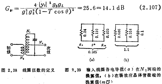
 . Suppose the admittance of the antenna is gA (set to 300Ω), and the number of turns of the coil is as specified in Figure 2.38, which is determined by the following two equations

可算得N1/N2=3.7,N1/N3=1.7。输入回路中的各电导分量,换算到线圈N1两端的值和换算到场效应晶体管的栅端的值如图2.39所示。Ciss=4.5pF换算成N1两端的值为1.58pF。
在此条件下,输入端的电压驻波比为0.24/0.145=1.66,是在容许范围内。
设斯忒恩的稳定系数为4,则由下式

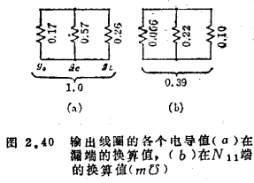
get . Because the load tuning admittance at the output is
 , So the turns ratio
 , The converted value of each conductance is shown in Figure 2.40. The insertion loss of the output coil is
 . From the formula (2.72), the gain is (including the insertion loss of the coil)
This is sufficient for high-frequency amplification stages. When removing the antenna from this system, replace g1 with g1-gA(N1/N3)2, then s is 1.5, so it is stable. The circuit including the bias is shown in Figure 2.41.
When constructing the actual circuit, pay special attention to keeping the stray capacitance between the input and output to a minimum, so as not to cause the circuit to fail.
stable.
●)In the product catalog data, it is 0.13pF, and 0.2pF has a certain margin.
Contact: Mr. Zou
Contact number: 0755-83888366-8022
Mobile phone: 18123972950
QQ: 2880195519
Contact Address: 5C1, Block CD, Tianji Building, Tianan Digital City, Chegongmiao, Futian District, Shenzhen
Please search WeChat official account: "KIA Semiconductor" or scan the following picture to "Follow" official WeChat official account
Please "follow" the official WeChat account: provide MOS tube technical assistance


