Electronic Technology Forum
Design and Principle of MOS Field Effect Transistor Band Pass Amplifier Circuit
For simplicity, take a single-tuned amplifier circuit as an example, and use the most common y parameter notation to illustrate the design basis of a band-pass amplifier (tuned amplifier)-stability, gain, and frequency characteristics.
(1) The stability of the amplifier
Figure 2.24 is a schematic diagram of a single-stage amplifier that uses a single-tuned loop in both the input part and the output part. Here the following formula holds.

In the formula, y1 and y2 are the admittance of single-tuned loop (omit the corner note) and can be written
●)Give Gma's Г s, Г L

This value is not an invariant in parameter substitution. Another expression of Gma is (2.55).


Substitute the tuning angle frequency And loop
 , Then y can be expressed as

x is the normalized detuning rate ●), which is generally equal to 。
。
In Figure 2.24, in order to make the amplification system stable, the real part of the input admittance yin of the entire network should take a positive value. If i2=0, yin can be given by the following formula.

suppose the phase angle of is θ, and the stable condition can be expressed as

When the frequency changes near fo, and thus x also changes, we can see from the vector trajectory of the second term ●●),

S is called Steyn's stability coefficient. The condition (2.39) has the same content as the K greater than 1 shown in the formula (2.21). s represents the ratio of the feedback voltage required for oscillation to the actual feedback voltage, which is not an invariant in parameter replacement. Design of MOS tube band-pass amplifier. The input and output of the amplifier have different tuning frequencies, and their respective Q values are also different. In addition, in the case of multiple tuning, it has a wider stable range than equation (2.39), so it is safer to judge with equation (2.39). In the actual amplifier, in order to prevent the instability caused by the deviation of the device and circuit parameters or due to the relationship of the frequency characteristics (see this page), s should be greater than 4.
●) In the narrow frequency band near fo, β can be approximated as

●●) The same result can be obtained by using the condition that the real part image.png of the output admittance is positive.
The input admittance when yT is not 0 can be expressed by equation (2.37), so when the tuning frequency of the output circuit x2=0, there is

In order to eliminate the imaginary part that appears at the input, the susceptance part whose value is j ▏yfyT▕ sinθ/g2 is added. In other words, tuning compensation must be performed ●). In the future, this tuned and compensated amplifier will be the subject of discussion.
(2) Conversion gain
If the symbol in the previous section is used to rewrite the conversion gain expression (2.27) with the y parameter, then there is

Where

δ is an item representing frequency characteristics ●●).

●)It is the same as the output compensation when the input is tuned.
●●)It is assumed that the y parameter does not change in the frequency bank under consideration.

Where Gam is the maximum usable gain when yT is ignored, image.png is the mismatch loss, image.png is the insertion loss of the tuning loop ●), and image.png is the feedback effect.
At the center frequency fo,

 for
for

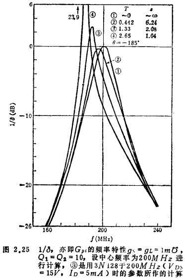
1/δ frequency characteristic, when T is changed, the calculation example is shown in Figure 2.25. Design of MOS tube band-pass amplifier. The S value is also marked in the figure. As T increases and S becomes smaller, it deviates from the center frequency and loses symmetry. In this sense, the 1/S value is sometimes called the deviation factor.
(3) Maximum available gain
When ensuring the absolute stability of the device, in order to obtain Gma, the admittance of the signal source and the load are accepted.

Calculate under the condition of input and output conjugate matching. at this time
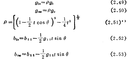
Where

Gma can also be expressed by the following formula (assuming that the matching circuit is lossless)

(4) How to stabilize the amplifier ●●)
When the device has potential instability, in order to make it stable, there are methods to neutralize and weaken the feedback and methods to make the input and output mismatch.
The most commonly used method is the y parameter neutralization method. When yT is in the third quadrant, the phase of the output is inverted and fed back to the input terminal via the neutralization element Y (refer to Figure 2.26(a)).
If Y is set to

(N is the turns ratio of the output coil), the y parameter including the neutralization circuit is
●)The meaningful situation of this formula is: image.png, that is, the device is in an absolutely stable state.
●●)Here again, the loss of the matching circuit is ignored.

and

The value of n at the maximum Gma is

In addition, it is the neutralization condition in the bridge circuit shown in Figure 2.26(b).

An example of using the mismatch method to achieve stability is Rathi's method 12). Take S as a constant value to design the largest . According to the results, when the input and output mismatch is of the same magnitude, the maximum
 the 1+m value is


at this time, Writable

 (The inherent stability factor of the device) (2.65)
Where

and

Is by the equation

The best value of the real root given. In the literature (12), there are graphs to show The functional relationship.
(5) Multi-stage amplifier
The conversion gain of the multi-stage amplifier composed of n stages is the product of the conversion gain of the first stage and the power gain of the subsequent stages.

Power gain given by the equation (2.26) when tuning

In the first level, Value and the conversion power gain of the input circuit
 (When tuning)

Multiply, you have

It is equal to the result obtained by formula (2.41).
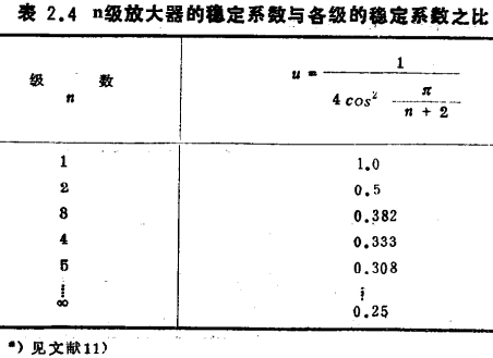
Regarding the issue of stability, when analyzing with loop gain as the core ●), in order to obtain stable amplification, an appropriate level of stability coefficient should be selected. Design of MOS tube band-pass amplifier. The multi-stage stability coefficient is the first-stage stability coefficient divided by the value u shown in Table 2.4.
(6) Frequency characteristics of single-tuned selection loop
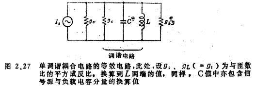
The single-tuned selective coupling circuit shown in Figure 2.27 is based on the following two formulas.
Transmission efficiency:

Insertion loss of tuning loop:

Where
QL is the loaded Q, Q=ωL (gs+gc+gL) (2.75)
Qu is Q without load, Q=ωLgc (2.76)
Mismatch loss:
m: mismatch ratio

Phase change:
-3dB bandwidth B can be obtained by formula (2.73) as

When the amplifying component is connected to an n-level amplifier, the total bandwidth B is 3dB. The relationship with B at all levels is

The QL of each level is (refer to Figure 2.28)


●)Here, suppose gs and gL are inversely proportional to the square of the ratio of the number of coil pitches, converted to the converted values at both ends of C. It is assumed that the value of C includes the converted value of the capacitance component of the signal source and the load. fo, x, namely
 ,
, . In addition, when considering the selectivity of the tuning loop, that is, the selectivity of the amplification system, it is assumed that the feedback has no effect.
(7) Characteristics of multiple tuning loop
Compared with the single-tuned loop, the complex tuning loop can get flat in the frequency band and steeply drop outside the frequency band. Its basic form is M coupling type and C coupling type shown in Figure 2.29.

Suppose gp, Cp, gs, and Cs in the figure are the converted values of the input and output admittance of the device connected to this loop at both ends of Lp and Ls. The coupling coefficient k is defined as

If the resonance frequency ωo is selected as

(For M coupling, replace Cp and Cs with Cp+Cm, Cs+Cm), the y parameter of this network is

Where

The resulting input and output admittance is


The conversion impedance Zo is

Such as calculating the amplitude characteristic of 1/Zo, when

When, it exhibits maximum flatness (critical coupling), less than this value is a unimodal characteristic,
 When it is larger than it, it has a bimodal characteristic.
Especially when Qp=Qs=Q,

The amplitude flatness characteristics are given, and the delay flatness characteristics are also given.

Figure 2.30 shows the amplitude characteristics when Qp=Qs.

The transmission efficiency of this coupling loop can be calculated from the following equation by calculating the conversion power gain


(8) "L"-shaped reactance bonding circuit
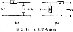
As shown in Figure 2.31, the "L"-shaped matching circuit is connected with pure reactance components. Due to its simple structure, it is suitable for use as a test circuit or at a fixed frequency. There are more than two types of networks that transform the admittance of any frequency into other arbitrary admittance. Any one of them can be selected according to the requirements of frequency characteristics.
The "L"-shaped coupling circuit is designed with the Smith chart showing impedance and admittance shown in Figure 2.32(a), which is extremely convenient. As shown in Figure 2.32, there are two types of circuits that transform the characteristic impedance of 50Ω into 1kΩ. The characteristics of these two circuits are similar near the center frequency, but the deviation from this frequency is very different. ①It becomes a high-pass type, ② It becomes a low-pass type, which can be selected according to requirements. Design of MOS tube band-pass amplifier. There are many similar coupling methods (for example, impedance transformation method with c division, etc.), please refer to other books for details.
Some basic knowledge is described above, and the different design methods used for different purposes are described below.

Contact: Mr. Zou
Contact number: 0755-83888366-8022
Mobile phone: 18123972950
QQ: 2880195519
Contact Address: 5C1, Block CD, Tianji Building, Tianan Digital City, Chegongmiao, Futian District, Shenzhen
Please search WeChat official account: "KIA Semiconductor" or scan the following picture to "Follow" official WeChat official account
Please "follow" the official WeChat account: provide MOS tube technical assistance


