Electronic Technology Forum
Analysis of the relationship between characteristic voltage of MOS field effect transistor weak voltage amplifier circuit
For example, the signal source resistance Rs is 100MΩ, and the change part of Ig is 1×10-14A. From equation (2.154), it can be seen that the drift voltage generated by the gate current Ig is the product of the change part of Ig and the signal source resistance, which is 1x10-14 ×108Ω=1μV. Therefore, if Rg is less than tens of MΩ, Id can be ignored compared with the voltage drift υd.
Taken from the formula (2.144’) ,Obtainable
 ,The size of υd is equal to
 。If the equation (2.144') is differentiated to the temperature, we get

Where

Where q is the amount of electron charge (1.6×10⁻¹⁸ Coulombs), Cg is the gate capacitance per channel length, μ is the carrier mobility, L is the channel length, and nss is the carrier concentration at the SiO2-Si interface . MOS field effect transistor weak voltage amplifier circuit. Among them, the main factors that change with temperature are μ and nss, so if you substitute formula (2.159) into formula (2.158) and make it equal to zero, you have to convert to the temperature drift of the input
Generally, at the SiO2-Si interface, the electron density increases in direct proportion to the temperature, while the carrier mobility tends to decrease in inverse proportion to the temperature. Table 2.7 gives the average value of the temperature coefficient of the MOS field effect transistor trial-produced by the authors and the size of its standard deviation. In the N-channel depletion mode, the carriers are electrons, and their density increases in proportion to the temperature, so Vp increases in proportion to the temperature;
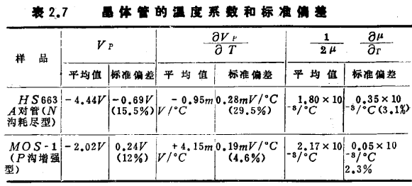
In the p-type channel, the carrier is a hole, which is offset by the increase of nss with temperature, so VT decreases inversely with temperature. In addition, in the N-type channel, VGS-Vp>0; in the P-type channel, VGS-Vp<0, the first and second terms on the right side of the formula (2.160) have mutually offset polarities, and the temperature drifts at that time Is zero.

Figure 2.96 shows the relationship between this temperature drift and VGS. Figure 2.96 (a) and (b) both show that the temperature drift υd is zero in the range of image.png. It is also known from the formula (2.160) that υd is directly proportional to VGS (gate DC bias).
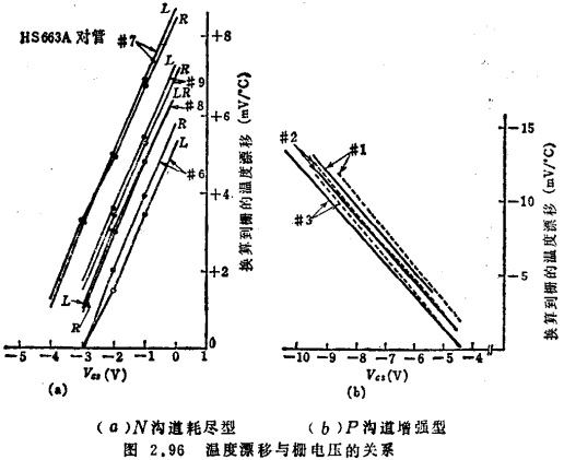
You can also use the method of adjusting VGS to the value shown in formula (2.161) to design a stable DC amplifier circuit, but in fact, considering the deviation of image.pngimage.png, etc., it is quite troublesome to adjust, so it is not practical . The practical low-drift circuit is still a differential amplifier circuit. At this time, the upper limit of the drift is restricted by the deviation of the device characteristics. MOS field effect transistor weak voltage amplifier circuit. The deviation of static characteristics can be seen from the deviation of IDO and Vp. From equation (2.159), it can be seen that the reasons for these deviations are μ, nss, L, Cg, etc. The measured IDO and Vp are related, as shown in Figure 2.97, the relationship is roughly as follows:
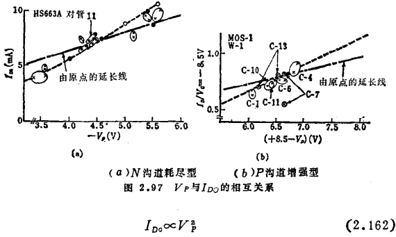
Therefore, the main cause of static characteristic deviation is nss.
On the other hand, the temperature drift of the differential amplifier circuit is the difference between the two devices υd, which can be given by equation (2.163).


After research by the author and others, it is found that for integrated circuit pair tubes, the magnitude of each drift item is roughly the same, and there is no correlation between each item (see Table 2.8).
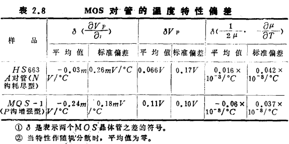
The total temperature drift is shown in Table 2.9, with

The relationship between integrated circuit and tube υd≌0.1~0.25 (mV/℃) (2.164). This drift level is much larger than the drift level of the paired (integrated circuit) bipolar transistors and junction field effect transistors used for differential amplification. MOS field effect transistor weak voltage amplifier circuit. However, if a stable mass production process is adopted and the device interval is designed to be as narrow as possible, the drift level of the MOS-to-tube can probably be improved to below 0.1mV/℃, with an average of about 0.05mV/℃.
Figure 2.98 is an example of a high input impedance amplifier using MOS field effect transistor integrated electrical devices. This device is composed of four integrated P-channel enhancement mode MOS field effect transistors, originally developed as a logic element in a desktop computer (see Figure 2.99 and Table 2.10).
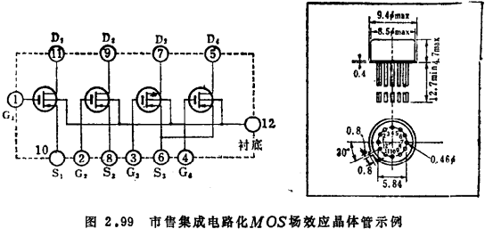
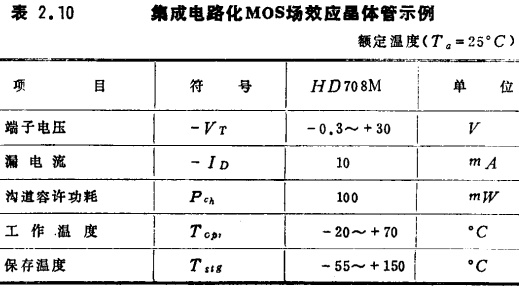
In the preamplifier, two tubes in HD708M are used for differential amplification, and the other two tubes are used as loads to form a cascaded amplifier circuit. Now suppose that the characteristics of the four MOS field effect transistors are equal, and their transconductance is gm. Because the resistance value of the load device is 1/gm, the voltage gain G1 of the preamplifier circuit is

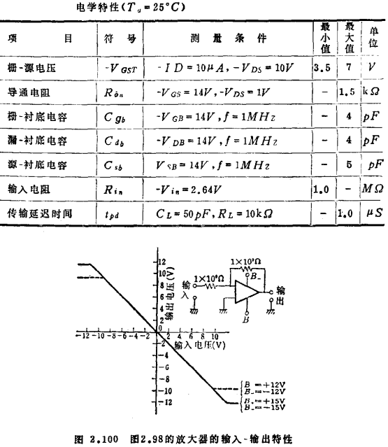
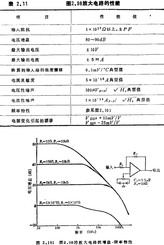
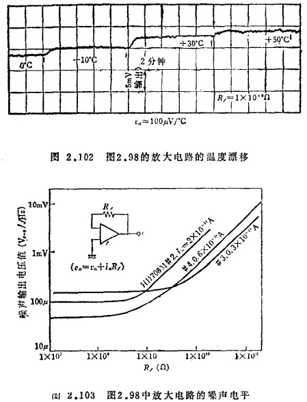
In other words, the preamplifier circuit can be used as an impedance converter here. The gate electrode of each MOS field effect transistor and the silicon substrate are connected with a Zener diode made by an integrated circuit method, which can prevent gate damage and characteristic changes caused by electrostatic induction and charging. On the other hand, due to the leakage current of the Zener diode, the input impedance, offset current, current noise, etc. have to be increased. Table 2.11 is its comprehensive performance. Figure 2.100 is the input-output characteristic, Figure 2.101 is the gain-frequency characteristic, Figure 2.102 is an example of temperature drift, and Figure 2.103 shows the relationship between the noise voltage and the negative feedback resistance Rf. MOS field effect transistor weak voltage amplifier circuit. In the formula (2.143’) in section 2.2.1, if Rs=Rf, the voltage noise can be separated from the measurement result And current noise in, respectively
 and
and 。
。
The design point of this circuit is that, because the input DC bias voltage of the integrated circuit operational amplifier in the main amplifier circuit is 0V, the output DC voltage of the preamplifier should also be set near 0V. In order to make the input voltage zero, the output voltage of the preamplifier is also roughly zero, R1 and R2 in Figure 2.98 should be set appropriately according to the power supply voltage.
The silicon substrate of HD708M is N-type. Because the P-N junction formed between the N-type substrate and the drain and source is not in a forward bias, the N-type substrate should be connected to the most positive potential point of the HD708M, that is, the Vs point in Figure 2.98. If the substrate potential is different, of course the ID~VGS characteristics will change under the influence of the substrate potential. Here, for the convenience of the design, the substrate potential is converted to the gate voltage VGS, and the conversion coefficient is obtained by experiment, and the design chart shown in Figure 2.104 is made. The usage of this diagram is to first determine the DC working current ID, get s from the ID-Is curve, and then get VD from the Vs-VD curve. When the power supply voltages Vss and VDD are higher than Vs and VD, insert step-down resistors R1 and R2 in their respective branches:
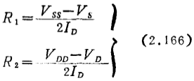
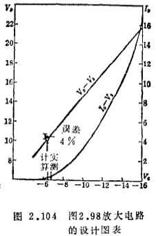
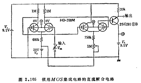
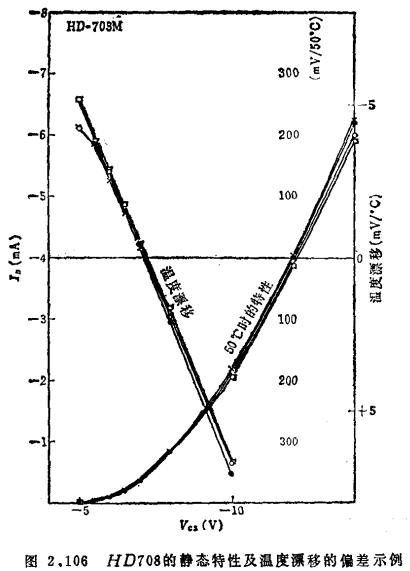
Figure 2.105 is another example of using MOS integrated circuit device HD708M. Here, because a HD708M integrated circuit can get a gain of more than 60dB, the whole circuit is designed according to the large load at low level. Figure 2.106 shows the deviation of static characteristics and temperature drift of four tubes in the same integrated circuit. Table 2.12 is the performance table of this amplifier.
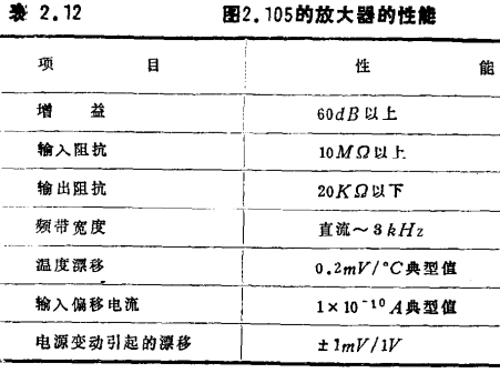
Compared with Table 2.11, the input offset current is larger, because the voltage between the silicon substrate and the gate is larger, and the leakage current of the Zener diode for gate protection increases.
Sometimes it is necessary to measure the voltage of a signal source with extremely high internal resistance. For example, PH (pH) meter, piezoelectric meter (crystal microphone and others, various detectors using ferroelectric medium and others), etc. are. In this case, the input impedance of the amplifier should be greater than the signal source impedance, so the circuit structure shown in Figure 2.86 (b) is often used. Figure 2.107(a) is another example that requires high input impedance 58). The pulse voltage (-40~100mV) generated by biological cells can be detected by inserting a tubular glass electrode filled with electrolyte into the cell with a diameter of about 1μ. MOS field effect transistor weak voltage amplifier circuit. Since the pulse width is about several ms, in order to detect and amplify this pulse voltage without distortion, a frequency bandwidth from DC to several kHz or more is required. But the internal resistance of this glass electrode is about 100MΩ, and the pulse width that should be observed is several milliseconds, so the amplifier must be a high-input impedance DC amplifier.
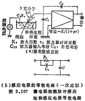
On the other hand, the tiny stray capacitance at the input terminal will cause significant distortion in the waveform of the induced pulse. Therefore, the input terminal capacitance, including the glass electrode capacitance and amplifier input capacitance, should be below 0.1pF. The negative capacitance formed by positive feedback can be used to compensate for the above capacitance. The compensation condition is that the negative capacitance (K-1) Cs converted to the input of the amplifier should be equal to the sum of the electrode capacitance C and the amplifier input capacitance Ci.

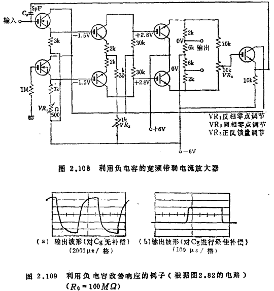
However, if the positive feedback compensation is excessive, the amplifier becomes unstable (oscillates). Figure 2.108 is a trial-produced amplifier circuit. In order to reduce the input capacitance and the leakage current from the input terminal to the cell, the front stage uses MOS field effect transistors, and the gain is stabilized by the source follower circuit. The second stage is a differential amplifier circuit of NPN transistors, and each emitter is connected to a 2kΩ resistor. The third stage is the differential circuit of the emitter follower. Therefore, in order to make the gain sufficiently stable, a polystyrene capacitor (5pF) with good insulation performance is connected between the output terminal and the input terminal to apply positive feedback. If compensated to the best condition, the original rise time can be improved to about 10μS, the improvement is about 200 times (see Figure 2.109).
Contact: Mr. Zou
Contact number: 0755-83888366-8022
Mobile phone: 18123972950
QQ: 2880195519
Contact Address: 5C1, Block CD, Tianji Building, Tianan Digital City, Chegongmiao, Futian District, Shenzhen
Please search WeChat official account: "KIA Semiconductor" or scan the following picture to "Follow" official WeChat official account
Please "follow" the official WeChat account: provide MOS tube technical assistance


