Electronic Technology Forum
Analyze the working relationship and characteristic classification of MOS field effect transistor DC bias circuit
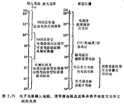
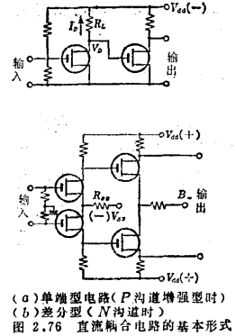
DC coupling amplifier circuit refers to a circuit that is directly coupled between the input stage, output stage, and stages, or coupled with resistors, Zener diodes, etc., and can be roughly divided into two types: single-ended (unbalanced) and differential as shown in Figure 2.76. Kind. The single-ended type, the drift caused by the change of the power supply voltage and the drift caused by the temperature change are relatively large, so it is rarely used for DC amplification. But it can be used in AC amplifier circuits that do not consider drift. On the contrary, the differential type has a drift compensation function, so the drift is small and the operating point is stable. It is not only suitable for DC amplifying circuits but also for AC amplifying circuits. It is very rare that the entire amplifying circuit is composed of field-effect transistors as shown in Figure 2.76. Most of them are based on the high input impedance of field-effect transistors. This type of device is only used in the primary stage. This is due to field-effect transistors and bipolar transistors. In comparison, the cost is high and the gain-bandwidth product is also small. MOS field effect transistor DC bias circuit. The gm of commercially available MOS field effect transistors is about image.png .Compared with ordinary bipolar transistors for small signal amplification, the silicon chip area is small, so the price is low. In order to increase the gain of the field effect transistor circuit, a large load resistance must be used, and the power supply voltage must be increased accordingly, and the bandwidth of the bandwidth is limited due to the negative feedback effect of the electrostatic capacitance CDG between the drain and the gate.
In principle, MOS transistors may have the four characteristics shown in Figure 2.77.
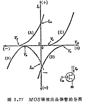
Currently, the commercially available products include (A) N-channel depletion type and (B) P-channel enhanced type. When the gate-source voltage VGS is zero, (A) has a current IDO flowing, while (B) is in an off state. For (B), the leakage current IDO under zero bias cannot be defined, but as shown by the dotted line in the figure, the characteristic curve (B) relative to the cut-off voltage Vp (pinch-off voltage) is made a symmetrical imaginary characteristic curve, such as imaginary The current value at the intersection of the characteristic curve and the ID axis is IDO, and the following characteristic expressions can be used for both types of transistors.

式中

gmfor

versus directly proportional. In other words, if the ID is lowered, the gm is also lowered. When a field effect transistor is also used in the secondary, if the power supply voltage is constant, the load resistance connected to the drain can increase inversely proportional to the ID, so as the ID is lowered, a larger voltage gain can be obtained. For example, for the primary circuit of Figure 2.76(a), if the power supply voltage VB and the drain voltage VD are given, there is

Therefore, from equations (2.146) and (2.147), the voltage gain is

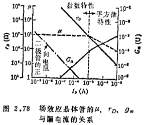
Obviously, in order to achieve high gain, it is advisable to work at a low level 49). The actual condition that restricts the increase in gain is that with the low level, the noise will increase and the bandwidth will also be narrowed due to the aforementioned dense effect. In addition, when using a polar transistor for the secondary, the higher the gm, the better, so it is better to increase the ID. If the ID is extremely reduced, the formula (2.144') will not hold. MOS field effect transistor DC bias circuit. The reason is that if the channel is pinched off, the majority carriers carrying the current disappear, and the minority carriers become the current carriers. Therefore, at this time, ID and the gate voltage have an exponential function relationship (50). General commodity field effect transistors, with For the boundary, from the square law characteristic of formula (2.144') to the exponential characteristic of formula (2.149).

Figure 2.78 is an example of the relationship between gm, μ (voltage amplification factor) and image.png (leakage resistance) and ID of a field effect transistor. In the figure, ID=10μA is used as the boundary to change from the square-law characteristic to the exponential characteristic.
Field-effect transistors, like vacuum tubes or bipolar transistors, have three grounding forms (see Figure 2.79). In order to obtain sufficient amplification, the amplifying circuit should be operated in the saturation region of the VD-ID characteristic.
For the ID-VD characteristics of Figure 2.80(a), the saturation zone is on the right side of the dotted line. In this area

The leakage current IDv can be obtained by equation (2.144’).
As shown in Figure 2.79(b) and (c), when the bias resistor Rss is connected to the source end, the formula (2.144') and

The VGS required to obtain the specified ID can be obtained, but this method is not as simple as the graphical method shown in Figure 2.80(b). This figure shows the case of N-channel depletion mode. If it is a differential amplifier circuit (Figure 2.76(b)), both IDs flow into Rss, so take 1/2 of the Rss value obtained from Figure 2.80(b).
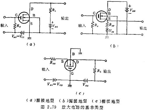
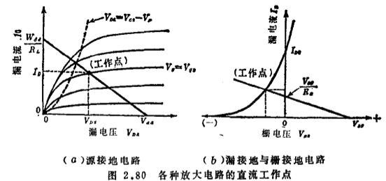
For reference, the voltage gain and output impedance of various grounding types are listed in Table 2.6, and the characteristics of commercial MOS transistors are listed in Figure 2.81.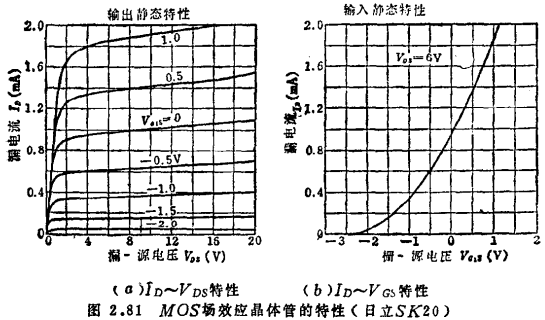
Figure 2.82 is an example of an AC amplifier circuit.
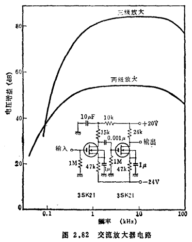
The leakage current is roughly specified as
 .If it is a three-stage amplification, a cascade circuit is also required.
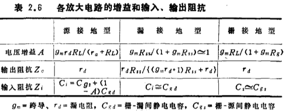
Figure 2.83 is a typical cascade method of MOS transistors and bipolar transistors.
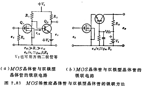
The figure (a) is the cascade of the source grounding type and the emitter grounding type, (b) is another cascading form. If (a) the input impedance ri2 of the bipolar transistor is much smaller than R1, then its voltage gain Gυ is

Where
gm is the transconductance of the field effect transistor
image.png is the current amplification factor of the bipolar transistor
In the case of (b)

The gain is the same as the case without bipolar transistors, but the impedance seen from the leakage of the field effect transistor is low, so it is suitable for high-frequency circuits. The cascade circuit integrated by field effect transistors is a quadrupole field effect transistor, as shown in Figure 2.84(b). Figure 2.84 (a) is its equivalent circuit and cascade method.
Figure 2.85 is an example of an integrated circuit cascaded audio amplifier, with an output power of 1W and a bandwidth of 0.1Hz~100kHz (51). Q1 and Q2 in Fig. 2.83(a) correspond to Q1 and Q2 in Fig. 2.85 respectively, R1 corresponds to the internal collector resistance of Q4, and R2 corresponds to Q6 (two diodes connected back to back). MOS field effect transistor DC bias circuit. Q3 and D1 are the DC bias components of Q4. Q7 to Q11 are quasi-complementary push-pull emitter follower circuits with a gain of 1. Thus, suppose the transconductance of Q1 is gm, and the current amplification factor of Q2 is , Then the gain G of the entire circuit is the same as formula (2.152), which can be written as

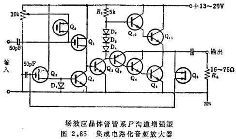
The reason for using field-effect transistors in the primary and bipolar transistors in the secondary is that a small capacitance integrated circuit capacitor (50pF) can be used to obtain a large input coupling circuit time constant, which prevents the decrease of low-frequency gain; the output circuit is saturated A bipolar transistor with a small resistance can improve power efficiency. Q5 is used as a DC negative feedback resistor for a stable operating point, and the internal resistance of Q4 is controlled by changing the internal resistance of Q3.
Contact: Mr. Zou
Contact number: 0755-83888366-8022
Mobile phone: 18123972950
QQ: 2880195519
Contact Address: 5C1, Block CD, Tianji Building, Tianan Digital City, Chegongmiao, Futian District, Shenzhen
Please search WeChat official account: "KIA Semiconductor" or scan the following picture to "Follow" official WeChat official account
Please "follow" the official WeChat account: provide MOS tube technical assistance


