Electronic Technology Forum
Overview and analysis of MOS transistor DC and low-frequency amplifier circuits
The DC amplifier circuit is roughly divided into the DC coupling circuit described in section 2.2.2 and the modulation type amplifier circuit described in section 2.2.5. Appropriately giving the high-end frequency pass characteristics to the DC amplifier circuit can form a low-frequency amplifier circuit. For example, the CR coupling circuit and the variable transformer coupling circuit are inserted between the input end, the output end and the stage, or the negative feedback of the double T circuit is inserted. Therefore, the basis of this type of circuit is a DC amplifier circuit. MOS transistor DC and low frequency amplifier circuit. Modulation type amplifier circuit is more complicated in circuit structure, and the bandwidth is restricted by the modulation frequency used, so it can only be used for a few The following weak signal amplification that requires good signal-to-noise ratio.
In the field of DC and low-frequency amplifying circuits, MOS transistors have high input impedance compared with amplifying components such as bipolar transistors, vacuum tubes, and junction field effect transistors, and are also most suitable for weak current amplification. The input impedance is a few hundred
In the following applications, MOS transistors are rarely used because of the low noise of bipolar transistors, the large gain under the similar die size, and the low price.
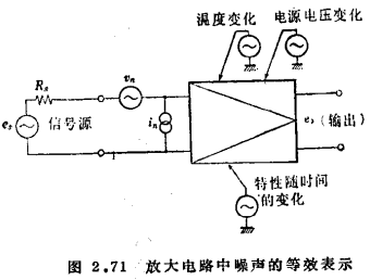
Figure 2.71 is a general representation that converts the noise of the amplifier circuit to the input. υn is the equivalent noise voltage source, and in is the equivalent noise current source. input signal , When the signal source impedance Rs is added to the amplifying circuit, such as
 Convert to signal
 ,then
,then the size can be expressed as

●)Original Chinese(2.143)、(2.144)、(2.145)The number is repeated, so the following three formulas are added To show the difference-translator's note.
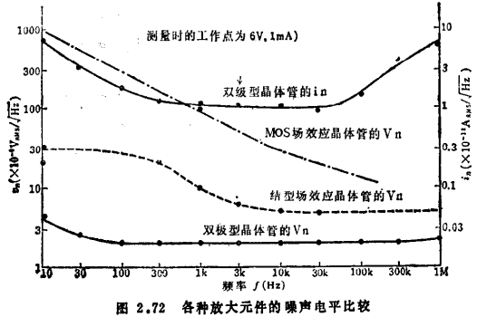
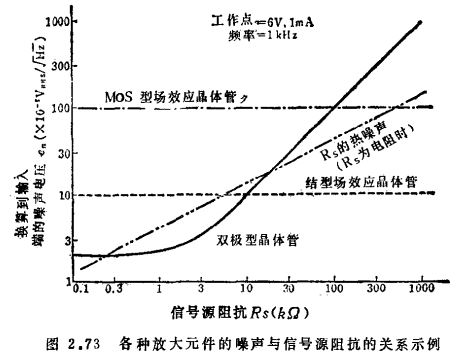
So as When υn plays a decisive role, on the contrary, when the situation is Rs>υn/in, inRs plays a decisive role. Figure 2.72 is a comparative example of the noise spectrum of a low-noise bipolar transistor, a common junction field effect transistor, and a MOS field effect transistor. The in of the two field effect transistors is too small to be measured. However, the i of the bipolar transistor obviously cannot be ignored. Figure 2.73 shows the relationship between the noise of these devices at 1kHz and the signal source impedance (Rs), which follows the relationship of equation (2.143). When Rs is below 10kΩ, bipolar transistors have the lowest noise. However, when it is above 10kΩ, the noise level of the junction field effect transistor will be exceeded, and when it is above 100kΩ, it will exceed the noise level of the MOS transistor. MOS transistor DC and low frequency amplifier circuit. In the figure, two dotted dotted lines are used to indicate the thermal noise of Rs. When Rs is greater than 500kΩ, its noise level has exceeded the noise level of the MOS field effect transistor, so the noise of the MOS transistor itself is no longer the main one. In other words, NF (noise figure) is almost close to 0dB.

In addition to noise, the DC amplifier circuit also has a drift problem. The so-called drift is zero-point drift, that is, the value of the DC drift of the output voltage converted to the input terminal when there is no signal, which is generally much larger than the aforementioned random noise.
The cause of the drift is the temperature change, the power supply voltage change, and the characteristic change over time as shown in Figure 2.71, and so on. Among the problems are temperature drift and drift over time, but the latter kind of drift has been significantly improved with the progress of the manufacturing process, so the former kind of drift is problematic.


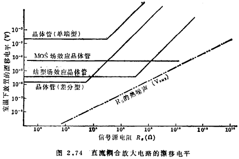
This kind of drift can also be equivalently expressed by a voltage source (υd) and a current source (id) like noise. Figure 2.74 shows the relationship between the drift and the signal source resistance. Compared with Figure 2.73, it can be found that the drift has the same tendency as random noise. The drift caused by id of the bipolar transistor, when Rs is at a few The above is the main one. Correspondingly, the id of the junction field effect transistor, when Rs is at a few
 Above, or the id of the MOS transistor, when Rs is several hundred
 The above is not a problem. MOS transistor DC and low frequency amplifier circuit. This is because the id of the bipolar transistor is the amount of change in the base current, while the id of the junction field effect transistor is the amount of change in the leakage current of the gate PN junction, and the id of the MOS transistor is the amount of change in the leakage current of the silicon dioxide film. .
According to the above discussion, what is the signal source resistance of the MOS transistor as a DC and low-frequency amplifying element The above areas have lower noise and are the most stable ●).

2.75 The corresponding relationship between the input resistance of scientific research, industrial measurement and other instruments and the input amplifiers and DC-AC converters used in these instruments is given. It can be seen that MOS transistors are used in circuits with the highest input impedance.
Contact: Mr. Zou
Contact number: 0755-83888366-8022
Mobile phone: 18123972950
QQ: 2880195519
Contact Address: 5C1, Block CD, Tianji Building, Tianan Digital City, Chegongmiao, Futian District, Shenzhen
Please search WeChat official account: "KIA Semiconductor" or scan the following picture to "Follow" official WeChat official account
Please "follow" the official WeChat account: provide MOS tube technical assistance


