Electronic Technology Forum
NMOS process conditions and steps, detailed explanations of advantages and disadvantages
In the development process of MOS circuits, the earliest and fastest development is PMOS integrated circuits. The production of PMOS circuits is basically a silicon planar process, usually called MOS conventional process. It has the advantages of simple process, uncomplicated equipment and easy control. However, PMOS circuits have the outstanding shortcoming of too low speed, which brings great difficulties to the development of high-speed, high-performance MOS large-scale integrated circuits. PMOS process. In order to improve circuit speed and performance, scientists have carried out a series of innovations to MOS technology. Some new materials and processes are used. For example, using semiconductor materials with high mobility, NMOS and GaAsNOS integrated circuits have been developed; in order to reduce the gate-source and gate-drain capacitances, gate self-aligned MOS technology has been developed; in terms of insulated gate dielectrics, compared to SiO span>2, better performance Si3N4, Al2O span>3, and other insulating films; the gate electrode of the device is in addition to the well-known aluminum gate , And developed silicon coarse and aluminum gates; in the formation of source and drain, and adjusting the threshold voltage of the device, the positive and negative aspects, the ion implantation technology is adopted. PMOS process. In this way, the MOS integrated circuit process greatly exceeds the scope of the silicon planar process, showing the new characteristics of the MOS process. This chapter mainly introduces NNOS: CMOS process and some new processes and new technologies used in these processes.
First, NMOS process
The N-channel process is an earlier choice for MOS circuits, because theoretically, the electron mobility is much higher and can be made into large transconductance MOS devices. NMOS process. However, due to the presence of positive charges at the interface of Si-SiO2, it is easy to cause N-channel depletion Type, but it is more difficult to make an N-channel enhancement type. Therefore, the early development speed is not as good as the PMOS circuit, but it has outstanding advantages. With the development of MOS technology, NMOS has already occupied an important position in the current high-speed large-scale MOS integrated circuits.
1. Advantages of NMOS
NMOS circuits have many advantages, which can be roughly summarized as follows:
(1) High switching speed
The switching speed of MOS integrated circuits and the equivalent time constant of charging and discharging devices Related. If
  is small, the speed of the circuit will be faster, starting from the second chapter Known from the discussion of the switch response of the phaser;
 < /span>
where . Because the mobility of electrons is about three times that of holes, if other parameters are the same, then
 should be
  triples, so
  Yes
Yes , the capacitance of N-channel MOS devices can be seen
  The charge and discharge speed is faster than that of P-channel MOS devices, so the open-channel MOS devices of the circuit are faster, so the switching speed of the circuit is high.
(2) Low threshold voltage
Because of the positive charge in SiO2, it is easy to produce N-channel depletion type, but it can Take certain measures to make VT move from a negative value to a positive value to obtain a smaller positive valueVT value. NMOS process. Therefore, the threshold voltage of N-channel enhancement type devices must be relatively low, so that they can work under low power supply. On the one hand, it can reduce power consumption, and on the other hand, it can be directly compatible with bipolar TTL circuits.

(3) It is beneficial to improve the integration level
Because the electron mobility is higher than the hole mobility, if you take  , for circuits with the same performance, N-channel devices can obtain a smaller design size, so that the circuit has a higher degree of integration, which is beneficial to reduce costs.
2. How to obtain N-channel enhanced devices
To manufacture N-channel enhanced devices, certain conditions must be created, and certain methods must be used to control the threshold voltage . NMOS process. The conditions and methods for realizing N-channel enhancement devices are discussed below.
(1) Making N-channel devices with high-concentration substrates
As discussed earlier, to realize N-channel enhanced devices, it must meet:

After moving items, get:
 < span style="font-size: 16px;">(6-1)
This is the substrate doping charge to realize the N-channel enhanced device .
.
In order to obtain the lowest surface state density, we use the<100>direction P-type Si single crystal,  Controlled in
 .
.
For typical doping concentrations , you can estimate the work function difference and the strong inverse surface potential
 is
is  .
.
If
Substituting the above data into equation (6-1), we get:

According to , Can be counted as:
 , The resistivity of the material must be less than 4Ω·cm.
If you want to get the threshold voltage The enhanced device can be calculated according to the expression of VT:

It can be seen that in order to realize N-channel enhanced devices, the use of high-concentration P-type substrates is a feasible method. NMOS process. However, to use  , take
  , which is
 Only 10V, which is relatively low.
(2) Substrate offset method
From the first chapter, we know that when a bias voltage is applied between the source and the substrate, an additional threshold voltage can be generated for the MOS device. . NMOS process. Known by the additional threshold voltage expression, there are three effects
  Factors, namely
  ,
,  and
and  . Therefore, just add a larger
  to make
  , and you can also appropriately reduce
  and
and  to improve
  and speed.

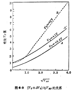
Figure 6-2 shows that N-channel devices are effective and the back grid bias
  Relationship.
Curve (A) represents the doping concentration of the substrate
 (reasonable pressure resistance)、

 (
( ).
).
Curve (B) means  , other conditions are the same as (A).
The curve (A') is pre-added (other conditions are the same as (A)),
  . Actually translate the curve (A) to the left by 1V, and you get (A').
If starting N-channel device, apply the bias of
  , effective The
  can reach 5V. Visibly apply
  to control N channel
 has obvious effect. NMOS process. In the actual circuit, in order to obtain a reasonable
  , Need to apply an additional power convenient.
Contact: Mr. Zou
Tel: 0755-83888366-8022
Mobile: 18123972950
QQ: 2880195519
Address: 5C1, CD Block, Tianji Building, Tian’an Digital City, Chegongmiao, Futian District, Shenzhen
Please search the WeChat official account: "KIA Semiconductor" or scan the picture below to "Follow" the official WeChat official account
Please "follow" the official WeChat account: provide MOS tube technical assistance


