Electronic Technology Forum
PMOS integrated circuit layout device design basis and detailed explanation
The design of MOS integrated circuits should generally include logic design, device design, layout design and process design. If the circuit diagram has been given, the task of designing is to determine the size of each device in the circuit (mainly the width and length of the channel), display the device graphics, layout, and draw a reasonable overall circuit layout (mask Composite version) and so on. The layout of the PMOS integrated circuit. In order to provide the photolithography mask used in the process and consider the process strip that can reach the circuit indexpieces.
The actual circuit design is more complicated. There are many important factors to consider, some of which are mutually restrictive. Therefore, the relationship between various factors must be handled well in the design to ensure that the various performances of the circuit meet the index requirements.
This chapter mainly introduces the basic principles of PMOS and CMOS integrated circuit design, as well as specific design methods and steps.
1. General design considerations
Before discussing design issues, first give some introduction to several issues that must be encountered in design.
(1) Circuit performance design range
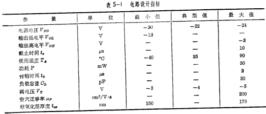
The circuit performance index is the basis for designing the circuit. Generally, it is proposed by the user according to the needs of the actual work. Table 5-1 lists the design performance indicators of a certain circuit, and the process parameters are also given.

The so-called design performance index refers to the circuit that is required to be designed, and its various performances and parameters must conform to the range specified by the index. For example: when requesting  , the output inverter of the circuit should be cut The time required to meet
  The power consumption of the circuit does not exceed 30mW, etc. , Otherwise the designed circuit is unqualified.
(2) The relationship between performance indicators and design parameters
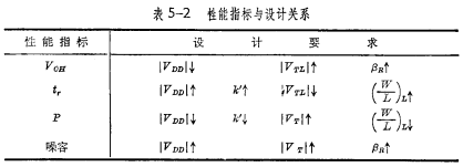
①Output high level For PMOS, formula (2-9) can be used for analysis.

Visible, to make  is close to zero, you must request
 .
.
②Deadline time According to formula (2-41), for PMOS, there are:

Visible, to make the switch fast, you must . If the power supply voltage and threshold voltage are given in advance, the geometric size of the designed load tube should be large, that is,
  .
.
③Power consumption P Power consumption . To make the power consumption of the circuit low, you must
  . The main purpose of the design is to make the channel geometry of the load tube as small as possible, that is,
④Anti-interference performance Can be expressed by cut-off and conduction tolerance The formula is analyzed. To make the circuit have strong anti-interference performance, you must require  Yes Given, the layout of the PMOS integrated circuit. Therefore, the geometric size ratio of the input tube and the load tube should be increased as much as possible during the design.
To sum up, it can be summarized in Table 5-2.

From the above analysis, it is known that the design requirements for power consumption and speed are contradictory. Starting from the power consumption, the size of the load tube should be small; starting from the speed, the size of the load tube should be large. Therefore, in the design, one should not only pursue a certain performance index and ignore other performances, but should distinguish the primary and secondary, and fully coordinate. The layout of the PMOS integrated circuit. The usual design is to determine the geometric size of the load device according to the speed requirements, and then verify whether it can meet the power consumption requirements. If not satisfied, the design parameters must be adjusted.
In the design, not only must deal with all kinds of contradictions, but also the relationship between theoretical design and actual process level, that is, the required performance indicators, process yield and The minimum strip width of the device must be adapted to the current actual process level to ensure that the production can reach a higher pass rate.
(3) Discussion of worst design conditions
In addition to dealing with the above-mentioned mutually restrictive factors, circuit design should also consider some disadvantages encountered in the actual work of the circuit. The layout of the PMOS integrated circuit. For example, the fluctuation of the power supply voltage, the increase of the ambient temperature and the fluctuation of the process parameters, etc., will all have an adverse effect on the performance of the circuit. Therefore, the worst condition should be considered when designing.
If the circuit can work normally under the worst conditions, then under normal conditions, the work of the circuit will of course be in a more ideal state.
The so-called worst-case condition means that the parameters used in the design are just the opposite of what is expected to improve the performance of the circuit. For example, the design of the load tube determines the switching speed of the circuit. For fast speed, then  , if you select
  will reduce the speed of the circuit, so this is the most important design of the load tube Bad conditions. Another example is the output tube design. The worst condition reflecting the high output level is high
 and low
  .
.
Next, we design the circuit according to the worst conditions.
2. Design of device channel width-to-length ratio
Any more complex MOS circuit can be broken down into many gate circuits, and the inverter is the most basic unit. The inverters can be divided into output inverters and internal inverters according to their location and function in the circuit. The layout of the PMOS integrated circuit. Therefore, the design of the channel geometry of each MOS tube in the entire circuit can be attributed to the design of the output inverter and internal inverter load tube and input tube geometric dimensions. The following discussion will take the common-fu leakage load MOS inverter as an example.
(1) Design of output inverter
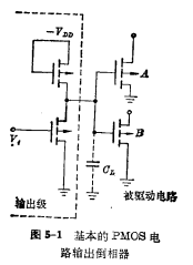
The output inverter of the circuit refers to the output circuit used to drive an external load, as shown in Figure 5-1. The output load includes the other two circuit pieces A, B and their interconnecting lines. When designing, it can be equivalent to a load capacitor .
.

①Load tube design The output inverter load tube design is generally determined by the cut-off time in the switching time of the circuit. Since the load tube is common-gate drain biased, it always works in the saturation region. According to the expression of the cut-off time of the saturated PMOS load inverter, the expression of the width-length ratio of the load tube can be obtained:

The following consider the value of each parameter in the formula (5-2).
a, The back gate effect should be considered. For PMOS, there are:

where In
In  and
and  , so you can take the average of the two:

So
b, Considering the design index gives the highest temperature
 , according to ( 1-71) formula, available:

c. The minimum power supply voltage is  , other parameters are based on the given indicators.
Substituting the data of the above formula into the formula (5-2), you can get:

②The design of the input tube The design of the input tube is generally determined by the static characteristics of the circuit (output high level). According to the formula (2-9):

Because:

where Input low level for the previous stage, so the calculation formula for the channel width-to-length ratio of the input device can be written:

Use the worst design conditions to get:

To sum up, the width-to-length ratio of the load tube of the output inverter is 1, and the width-to-length ratio of the input tube is 12. If the minimum size of the channel is 8μm, the sizes of the two tubes of the output inverter are:

③Output power verification
In MOS circuits, it is usually hoped that the output inverter can have a larger drive capacity, so the power dissipation is larger. In actual circuit design, the power dissipation calculated by the output stage is almost equal to the sum of other inverters in the circuit.
The power consumption of the output inverter can be calculated from the power consumption formula according to the design indicators given above and taking into account the worst design conditions:

The above calculation shows that the power consumption of the output inverter is about half of the total power consumption of the circuit. It can be seen that the ratio of the length of the load tube to 1 is appropriate.
If considering the actual working circuit, too high junction temperature will cause obvious leakage of PN junction and increase power consumption. Under the premise of not affecting the speed, it can make (W /L)L whichever is smaller.
(2) Internal inverter design
①Features of internal inverter
The so-called internal inverter refers to an inverter that only drives an internal load or a logic gate inside the circuit, as shown in Figure 5-2. The layout of the PMOS integrated circuit. The design process is basically the same as that of the output inverter, but in terms of design details, there are the following differences:
a. The speed of the internal inverter is generally determined by the specified maximum clock frequency, so the internal inverter requires a higher switching speed. Assuming that the deadline  can meet the clock frequency requirements, then the calculation is You can save
  .
.
b. The ability of the internal inverter to drive the load is not very demanding. Generally, an internal inverter only needs to drive 3~4 next-stage internal inverters, such as each Load capacitance  , the total load capacitance is 2pF.
c, the internal inverter output high and low level requirements are not high, output high level The requirements are not as strict as the output inverter, as long as the next stage can be cut off normally. So take:

where The noise voltage is generally 1V, so,

The low-level output requirements are also low, as long as the lower-level inverter can be turned on normally.
Next, we use the method of checking diagrams to design the internal inverter.
②Design of load tube
First write the voltage formula normalized to the maximum output voltage:

where (Lower requirements than the output inverter),
  .
.

So:
Check the chart (2-26),  .
.
Because:
The calculation formula for the aspect ratio can be written:

③The design of the input tube
The normalized input voltage is:

The normalized output voltage is:

Check the chart (2-15) to get , that is:

In actual design, often use  is smaller, so generally take
  as < img src="/userfiles/images/2020/11/19/2020111910472153.png" title="image.png" alt="image.png"/> The reciprocal, so take
  .
.
If the minimum width of the channel is still 8μm, the channel size of the internal inverter can be written as:

④Verification of speed
When designing the output inverter, the calculation of the input tube uses the low output high level , which ensures that the on-time is much shorter than the cut-off time. The layout of the PMOS integrated circuit. However, in the calculation of the input tube of the internal inverter, due to the higher high level
  , it does not necessarily guarantee that the on-time is less than the cut-off time. So it must be corrected by

 ,data to be verified, as guided Whether the open time can meet the requirement of less than 1μs.
The on-time is given by (2-36) formula:

The data of each parameter (taking into account the worst conditions) is:


Substitute into (2-36) formula, get:

Visible It is much smaller than the specified 1μs, so the above design data can fully meet the requirements of the internal inverter switching speed.
Contact: Mr. Zou
Tel: 0755-83888366-8022
Mobile: 18123972950
QQ: 2880195519
Address: 5C1, CD Block, Tianji Building, Tian’an Digital City, Chegongmiao, Futian District, Shenzhen
Please search WeChat Official Account: "KIA Semiconductor" or scan the following picture to "Follow" Official WeChat Official Account
Please "Follow" the official WeChat account: provide MOS tube technical assistance


