Electronic Technology Forum
Method of making PMOS layout design device
PMOS layout design
The layout design is based on the design requirements and process conditions, selecting the appropriate size, determining the device geometry, making reasonable layout and wiring, forming the overall circuit layout, and following the process The process designs a set of photolithography masks. Correct and good layout design is not only necessary to realize circuit functions, but also has a great influence on yield, integration and circuit performance. PMOS layout design
The layout design must consider three principles:
①Using the chip area most effectively;
②Ensure that the performance of all aspects of the circuit meets the requirements of the design index;
③Ensure a high yield rate.
In order to achieve these goals, various layout plans must be carefully studied and strive to achieve the best.
Currently, the layout design of medium and small-scale integrated circuits is often done manually based on practical experience, while the layout design of large-scale and very large-scale integrated circuits must be assisted by computers. Here are some introductions to the basic knowledge of the layout design of medium and small-scale integrated circuits.
1. Regulations on the basic size of the layout
When drawing a layout, the size of the drawing (including the size of the four-layer mask) must be carefully considered. From the perspective of improving integration, the size of the drawing is of course as small as possible, but it is limited by electrical performance and process level. The electrical performance limits generally refer to the drain-source breakdown characteristics of the device, the maximum current density of the aluminum lead, and the minimum gap between the diffusion bars that cause parasitic transistors, and so on. The limitation of the process level mainly refers to the plate-making accuracy, the previous process level and the registration accuracy of lithography. PMOS layout design. Of course, the size requirements are not static, but are continuously reduced with the improvement of the technological level. For example, in the earlier conventional PMOS process, the minimum channel length is generally designed to be 8~12μm, while the current advanced NMOS process, the channel length L has been reduced to about 2μm or even smaller.
The following are only the principles and regulations of the graphics size of the conventional PMOS process level, and some introductions are made separately for reference.
(1) Determination of the minimum channel size
The MOS device design mentioned above gives the tube width to length ratio. How to determine the minimum channel length L should be considered from three aspects.
a. The actual level of craftsmanship.
b. Source-drain punch-through voltage. As mentioned in the first chapter, L is shortened and the punch-through voltage  drops . In order to ensure that the source-drain punch-through voltage is greater than the operating voltage of the MOS tube, it is required to
  , If the substrate concentration
  , the minimum width of the channel is required to be:
 < /span>
Of course, the working voltage of the circuit is reduced,  can reduce the requirements, and L can be reduced.
c. Due to the influence of the lateral diffusion of the source and drain regions, the actual channel length will be smaller than the one drawn on the layout. Generally, the length of the horizontal diffusion is taken as the depth of the diffusion junction  , so the actual groove The length of the road should be:
 < /span>
If the junction depth is 2μm, the actual channel length is selected as 8μm, the source-drain distance should be 12μm when drawing the layout.
(2) General graphic size
① Drawing mark In order to make the drawing clear, distinguish the diffusion area, gate area, lead hole, aluminum lead strip and other four photolithographic mask patterns on the same drawing. Generally, different lines are used in each area. to mark. Figure 5-3 is the MOS circuit drawing mark issued by the Ministry in 1977.
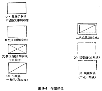
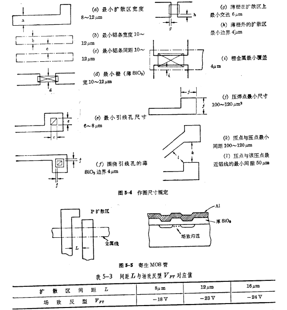
②Size requirements There are other graphics (or pressure points) and The minimum gap of the scribing area is 160~200μm; the distance between the two circuits is 520~600μm.
In Figure 5-4,  is the limitation on the circuit size of the later process, such as the size of the test probe and the hot-pressed solder joint, the area required for the test and the pressure-welded must be guaranteed; PMOS layout design. Another example is the use of a diamond knife to scribing, each circuit chip must have sufficient spacing; in addition, there must be a certain gap between the pressure point and the pressure point to ensure that the adjacent metal wires of the pressure welding point do not cause short circuits, etc. Wait.
(3) Selection of the spacing of the diffusion bars
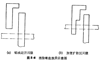
The diffusion area of the MOS circuit is mainly the drain area of the load tube (including the power diffusion area), the common diffusion area of the two inverter devices, and the source area of the input tube (including the ground Diffusion area) and the common diffusion area of two or three transistors, etc. In the layout, it is first hoped that the layout of the diffusion area can save the area of the wafer, so the diffusion area should be evenly and densely distributed on the wafer, and make full use of the common diffusion area. Secondly, the layout of the diffusion area (including the arrangement of the devices) should be conducive to the layout of the aluminum leads, so that the aluminum leads are evenly distributed on the layout without uneven density. Third, the layout of the diffusion area must also avoid parasitic effects. If the distance between the two diffusion bars is very close, when the aluminum wire passes through the thick oxide layer above the diffusion area, it will cause a "field inversion transistor", as shown in Figure 5-5. This parasitic effect will cause serious leakage or punch-through of the two diffusion regions, increase the power consumption of the circuit and affect the performance of the circuit.
The formation of field inversion transistors is related to the distance between the two diffusion regions. Because of its field inversion threshold voltage not only with the oxide layer The thickness is related to the distance L between the two diffusion regions (the actual L is the channel length of the parasitic transistor). The following table shows the values of
  for different labor values;
 < /span>
It can be seen that in some areas prone to parasitic effects, the distance between the two diffusion areas should be appropriately widened, with a minimum distance of 12μm. Since the formation of the channel is actually an asymptotic process, even if the voltage ratio is  If it is too small, there will still be channel leakage, so care must be taken in the design. PMOS layout design. To eliminate parasitic effects, the following two methods are usually used:
①Aluminum wire avoids the gap between the two diffusion areas;
②Enlarge the gap of the diffuser, as shown in Figure 5-6.
2, device graphics considerations
(1) General device graphics
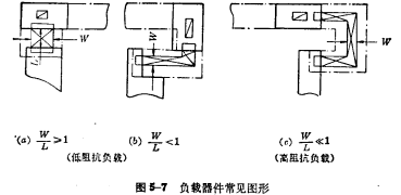
The graphic design of the device is inseparable from the layout of the diffusion area. For the two component sizes of the inverter in the circuit, there can be various patterns in the layout. Generally speaking, the graphics should be simple, occupying a small area, and the graphics should be conducive to the performance of the circuit.
For load devices with common gate drain, In the case of value > 1, the graph is very simple, as shown in Figure 5-7(a).
for In the case of value < 1, it can be flexibly designed according to the specific layout of the circuit. The commonly used graphics are shown in Figure 5-7 (b) and (c).
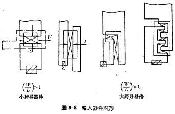
For the input device, the smaller size is very simple, and the larger-size graphics commonly have "L" and "comb" shapes, as shown in Figure 5-8.
(2) Gate protection device graphics
In the layout of the entire circuit, gate protection devices are also included. The first chapter introduces four forms of gate protection devices. Here are two commonly used gate protection device patterns for PMOS circuits.
Figure 5-9 shows the gate cover protection diode pattern. This device has a fairly long boundary, and a series diffusion resistor is added behind the diode to ensure a large current leakage capacity.
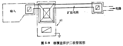
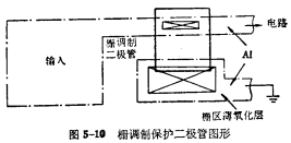
Figure 5-10 shows the gate modulation protection diode pattern.
For these two devices, a thin oxide layer with a grounded aluminum lead is prepared on the PN junction, which reduces the reverse breakdown voltage of the diode by 20~30V compared with ordinary diodes. , So the actual breakdown voltage is in the range of 40~60V.
 < /span>
3. Aluminum lead layout principles
The lead layout is commonly known as "wiring". After determining the position of each device in the circuit board, the aluminum leads are used to connect the devices according to the requirements of the circuit. This is Internal wiring; PMOS layout design. In addition, there are external wiring for input, output, power and ground voltage points.
Aluminum lead layout should generally pay attention to the following points:
① Parasitic effects should be avoided as much as possible. High-voltage lines (output point D) or power lines should generally be kept away from the source, drain and gate of the input device.
②The smaller the connection resistance, the better. The aluminum strip can be widened appropriately, generally 12~16μm can be used. In order to reduce the influence of lead resistance, aluminum wires are used as much as possible for power and ground wires. But when the aluminum wire cannot be used, the diffusion area can be used as the lead, but the lead hole must pay attention to the influence of the diffusion resistance on the circuit performance.
③Aluminum leads should try to avoid using long wires because the more places they cross, the more chances of pinholes and breakage. When it is unavoidable to use long leads, the width and thickness of the aluminum wire should be appropriately increased.
④The tunnel lead when two lines cross. The tunnel lead is also called the diffusion buried lead under the original oxide layer. As shown in Figure 5-11. Using tunnel leads, generally let the low voltage (such as the ground wire) lead out through the aluminum wire, so as to prevent the high voltage from causing undesirable leakage effects on the thin oxide layer. The high-voltage line is generally drawn from the diffusion line.
4. Draw a general picture
According to the given design index, the geometric dimensions of each device in the circuit are calculated, and then according to some basic principles and regulations of drawing, you can start to design and draw the circuit version Sub-total map (ie, mask composite map) to get the photolithography mask of the circuit.
(1) Typesetting sketchA circuit composite version with excellent performance, You can't draw it all at once. Before the formal drawing of the layout, a sketch of the circuit board must be drawn first.
The main purpose is: first, roughly arrange the position of each device; second, draw the connection pattern of the inner leads, and avoid the inner leads from crossing each other; Third, determine the direction of the input and output terminals. After getting a satisfactory layout. Then formally draw the general plan.
The following takes a 4×3 NAND gate PMOS circuit (positive logic regulation) produced by a certain factory as an example (as shown in Figure 5-12), for some brief introduction.
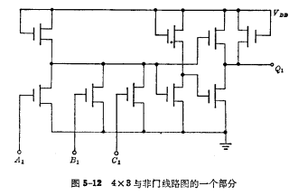
For all circuits, there must be input, output, power, and ground terminals. In this circuit, there are 4 groups of NAND gates, each group has 3 input terminals, 1 output terminal, plus a common power supply and ground terminal, so there are a total of 18 lead terminals.
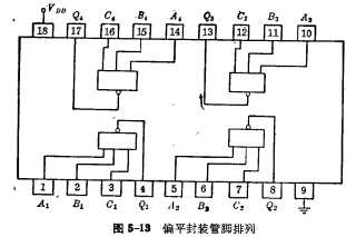
The arrangement of each terminal should be standardized. PMOS layout design. For the flat ceramic package, its pin arrangement and numbering are shown in Figure 5-13. In this P-channel series circuit, the power supply is connected to the 18th pin, and the ground wire is connected to the 9th pin. The input and output terminals are arranged as shown in the figure. This 4×3 NAND gate circuit is the same in each group, so as long as the positions of the tubes in a group are arranged, according to the principle of symmetry, the graphics of the four groups can be arranged in a complete version.
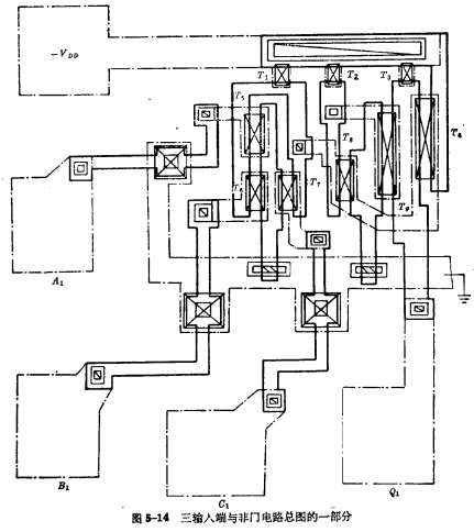
(2) Draw the layout sub-master map the version sub-master map ( That is, the mask composite map), according to the level of the plate-making process, a drawing scale of more than 200 times is generally used, because under such a magnification, the smallest size device can be accurately drawn. According to the layout sketch, the layout of the circuit is drawn on the coordinate paper to obtain the general layout. PMOS layout design. Figure 5-14 shows a quarter of the total diagram of the 4×3 NAND gate.
After the master plan is completed, it must be carefully checked and proofread, especially the following issues.
①Whether the device size is correct, and whether the various sizes meet the principle requirements;
②Whether the connection is correct, check it against the circuit;
③Whether there are missing points or lines, the version error is often forgot to open the lead hole or miss some connections;
④Whether there is a place where parasitic MOS transistors are generated;
⑤ Whether the arrangement of hot pressing points meets the packaging requirements.
After the general drawing is checked, the sub-map (lithography mask) can be engraved and used for plate making.
 < /span>
Contact: Mr. Zou
Tel: 0755-83888366-8022
Mobile: 18123972950
QQ: 2880195519
Contact address: 5C1, CD Block, Tianji Building, Tian’an Digital City, Chegongmiao, Futian District, Shenzhen
Please search the WeChat official account: "KIA Semiconductor" or scan the picture below to "Follow" the official WeChat official account
Please "follow" the official WeChat account: provide MOS tube technical assistance


