Electronic Technology Forum
CMOS circuit device design calculation method
First, CMOS circuit device design
To design CMOS circuits, in general, according to user requirements and given circuit indicators, first design each device in the circuit, then draw a published drawing, and finally determine the process parameter. This section mainly introduces CMOS circuit device design and layout design. CMOS circuit device.
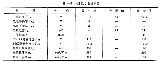
Since the inverter is the basis of the circuit, first consider the design of each component of the inverter. CMOS circuit device. In the design of CMOS inverters, the high-level and low-level requirements can be ignored. The main design indicators are the highest operating frequency and noise tolerance. The design indicators and process parameters are given in Table 5-4.

1, device size calculation
According to the given conditions, we can calculate from the working frequency. To achieve the best speed, you should select  , because
  , therefore:

In order to meet the requirements of the highest operating frequency, the rise and fall times are set to be smaller, assuming  .
.
In order to ensure that the circuit works well within the specified range, the "worst case" design should also be adopted. CMOS circuit device. For the operating frequency, low power supply voltage, high threshold voltage, thick oxide layer and large load capacitance are unfavorable factors, so the following data should be taken when calculating:

(1) Calculation of load pipe
First, write the normalized threshold voltage based on the worst-case data:

Calculate according to the formula (2-86):

According to (2-77) type , available:

Because , the width to length ratio of the load tube can be obtained:

(2) Input tube calculation
According to (2-82) formula:

So, it can be obtained:

by , the width to length ratio of the input tube is calculated as:

If If the channel length is 10 μm, the channel width of the load tube is 140 μm, and the channel width of the input tube is 60 μm.
If the calculated unit is a two-input NAND gate circuit, since the load tube is connected in parallel,  , so the channel width to length ratio of the two load tubes is the same as the size of the inverter load tube above; CMOS circuit device. The input tubes are connected in series,
  , so each input tube The aspect ratio should be twice that of the input tube of the inverter above.
2. Noise tolerance calculation
According to the definition of maximum noise capacity: High level maximum voice capacity , low-level maximum noise
  . Therefore, as long as the conversion level is calculated, the noise capacity is determined. CMOS circuit device. For the worst condition of high-level noise,
  , the conversion level can be calculated according to formula (2-68):

For the worst condition of low-level noise, , the conversion level is calculated as:

So, the high-level noise capacity is calculated as:

The low-level noise capacity is:

Can meet the design index noise capacity requirement of 3V.
3. Power consumption estimation
According to the formula (2-92), the power consumption is:

Contact: Mr. Zou
Tel: 0755-83888366-8022
Mobile: 18123972950
QQ: 2880195519
Address: 5C1, CD Block, Tianji Building, Tian’an Digital City, Chegongmiao, Futian District, Shenzhen
Please search WeChat Official Account: "KIA Semiconductor" or scan the following picture to "Follow" Official WeChat Official Account
请“关注”官方微信公众号:提供 MOS管 技术帮助


