Electronic Technology Forum
CMOS threshold voltage design device and process
To make the designed circuit layout meet the design index requirements in terms of performance, process design must be carried out to determine reasonable material parameters, process parameters and process conditions. Among them, the control of the threshold voltage is the core of the CMOS circuit process design. CMOS threshold voltage design. Because, on the one hand, it is necessary to ensure the enhanced work of the NMOS tube, that is,  ; On the other hand, the threshold voltages of NMOS and PMOS tubes are required to match as much as possible, that is,
  ; Many other material parameters and process parameters are based on
  are determined, so the design of the threshold voltage is mainly introduced here. As for the material parameters, process parameters and process conditions, they will be introduced separately in the next chapter.


1. Ensure that the NMOS tube is enhanced
As mentioned in the first chapter, to make the NMOS tube an enhanced work, you must require:

Therefore, measures must be taken in the process to reduce as much as possible and appropriately increase Qw, but the doping concentration of the P-well region
 can not be raised very high, it is subject to the breakdown voltage limit. CMOS threshold voltage design. According to the current process conditions,
  can be controlled in
  about; P-well doping The impurity concentration should be greater than
 .
.
2, VT matching
The CMOS circuit must have high anti-interference performance and good switching characteristics, and the threshold voltage of the two tubes must be well matched, namely:

From this condition, the following expression can be obtained:

So it can be solved:
The value in the brackets of the above formula is in  and
and  is usually a constant within a certain range; where
  is very small and usually has minimal impact on matching, while
  can be used by
 mainly uses
  as the variable.
From the above formula,  and
and  The perfect match condition will be
  and
and 
 Be sure,
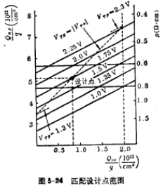
  From the figure, the following two points can be drawn:
①The setting of threshold voltage matching for N-channel and P-channel devicesThe counting point is on the matching line , for each matching design point, it is
  and
and  is a function of P-well diffusion concentration and surface charge.
②Visible from the matching line, when the surface charge is  is larger, a very high P- trap diffusion concentration is required. But this kind of extremely low resistivity P-type substrate diffusion is not easy to control, and high concentration diffusion will cause a serious decline in the electron mobility of N-channel devices; moreover, high
  makes P-channel devices
 Good match of threshold voltage.

To sum up, to make a CMOS circuit with a good threshold voltage matching, the process requirements are strict. Because for each design point on the matching line, there is only one  and
and  value, so CMOS process is the most sensitive process to circuit characteristics . CMOS threshold voltage design. For a specific CMOS process specification, it should be that the P- well diffusion sheet resistance value has good repeatability, and the gate oxide surface charge
  The value should be small and have good repeatability. Therefore, strict purification requirements are put forward for the CMOS process. Otherwise, it is difficult to achieve a perfect match.
Contact: Mr. Zou
Tel: 0755-83888366-8022
Mobile: 18123972950
QQ: 2880195519
Address: 5C1, CD Block, Tianji Building, Tian’an Digital City, Chegongmiao, Futian District, Shenzhen
Please search WeChat Official Account: "KIA Semiconductor" or scan the following picture to "Follow" Official WeChat Official Account
Please "Follow" the official WeChat account: provide MOS tube technical assistance


