Electronic Technology Forum
Introduction to the basic principles of VLSI design
I. Overview
The circuit design and layout mentioned above are all based on conventional process considerations, and are generally used for small and medium-sized MOS integrated circuits. The speed of MOS technology development is amazing. MOS integrated circuits are about to double every year in terms of performance and integration. In the 1970s, MOS chips have evolved from shift registers, gate circuits, and flip-flops with low speed (on the order of ms) and low integration to a relatively high speed (on the order of ns) with tens of thousands of components. The microprocessor chip. At the end of the 1970s, MOS technology has been developed towards N-channel VLSI with 5V single power supply. This circuit can execute complex calculation instructions in a cycle of less than 100ns, and achieve static and dynamic in less than 50ns. Storage operations, and the power consumption of these operations is extremely low. Very large scale integrated circuit design.
The common method for improving the performance and integration of MOS circuits is to shorten the effective channel length of the basic MOS FET or the spacing between the source and drain diffusion regions.
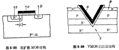
There are currently two ways to achieve a short channel: one is to rely on a double diffusion process, that is, to make a depletion type with a longer channel of 5μm under the MOS gate The series structure of the device and a 1μm short channel enhanced device, its effective channel length can be controlled by flip diffusion, as shown in Figure 5 25 shown. If the double-diffused structure pattern is vertical (as shown in Figure 5-26), it is VMOS. The surface of the VMOS transistor is located on the V-shaped groove surface obtained by anisotropic etching at the bottom of the silicon village. Both of these two types of double-diffused devices require a new process and a new circuit structure that are significantly different from the conventional silicon gate process.

Another way to shorten the channel is to directly scale down the size and performance parameters of the MOS device, that is, scale down the conventional N-channel silicon gate structure MOS device. Very large scale integrated circuit design. By scaling down the device, higher speed, integration and lower power consumption can be achieved. This section will outline the scaling principles applied in the design of large-scale and very large-scale integrated circuits.
2. Design principle of proportional reduction
Since Leiter applied the principle of scaling down to make high-performance MOS devices (HMOS) in 1977, this design principle has gradually become large-scale and super-largescale Guidelines for integrated circuit design have been widely used. Because it has the following outstanding advantages:
①The method of scaling down the size and parameters of the device is relatively simple and does not require any reform of the conventional process. Therefore, it is not necessary to increase the cost and give full play to the conventional process. Function, so that the original production experience can be quickly established on the production line.
②Because it is directly developed from the conventional process, there is no need to redesign the structure of the device, nor does it require a complicated circuit structure.
③With the improvement of photolithography and heat treatment processes and the adoption of fine processing techniques (such as electron beam exposure), the principle of scaling down is applicable to smaller and smaller circuit patterns. It is an ideal way to improve the design.
1. Shrinking principle
In order to design a relatively small channel length L devices, and maintain the appropriate threshold voltage and drain-source breakdown voltage, the theory that the device is scaled down, it is necessary to change three proportionally Variables, namely device size, voltage and substrate doping concentration.
First, reduce the total linear size of the device by S times (S>1). This reduction includes the vertical direction, such as the thickness of the gate insulation layer  junction depth
  and horizontal direction, such as channel lengthL, channel width W. Very large scale integrated circuit design. So, these new parameters constitute a new scaled-down device.
Secondly, the working voltage applied to the device is also reduced by the same scaling factor. Such as  .
.
Thirdly, to maintain proper threshold voltage and drain-source breakdown voltage, the doping concentration must be increased by S times, that is, 
 .
.
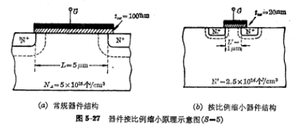
For example, Figure 5-27 shows a schematic diagram of the principle of scaling down. The figure (a) shows the device structure of conventional technology, its  . Figure (b) is a scaled-down device (set S=5), and its
  .
.

2. Circuit performance changes
After shrinking in accordance with the above principles, the performance of devices and circuits will also change significantly.
(1)Due to reduced voltage and increased impurity concentration, The width of the depletion layer shrinks as the device size shrinks, that is,  .
.
(2)Because of  is reduced by S times, so the threshold voltage is also reduced by S times in the same proportion, ie
 .
.
(3)The liner usually used in N-channel devices The bottom bias voltage can also be reduced accordingly.
(4) Voltage applied to source junction and drain junction The voltage drop, or the voltage drop applied to the depletion region under the gate, is reduced by a factor of S.
(5)All equations describing the characteristics of MOS FET devices, also It can be scaled down by S times, such as  .
.
(6)Because the voltage and current are both reduced by S times, Therefore, the power consumption is reduced by  times.
(7)The electrode spacing is reduced by S times, and the grid is insulated The layer is thinner and the width of the depletion layer is reduced, so the capacitance of all the circuit elements is reduced by S times. Therefore, the delay time of each circuit is also reduced by S times.
(8)The product of power and delay time is reduced times.
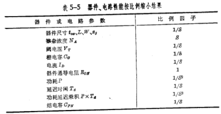
The circuit parameters of the above-mentioned scaled-down devices are summarized in Table 5-5. It can be seen that after the devices and circuits are scaled down, the circuit's integration, power consumption and speed have been greatly improved.
3, there is a problem
After the principle of scaling down was put forward, it greatly promoted the development of MOS integrated circuits, but it still has some unsolved problems. Very large scale integrated circuit design. For example, in the sub-threshold region (before the formation of the MOS inversion channel) or the weak inversion region, the device parameters cannot be scaled down, so the source-drain leakage current in the sub-threshold region cannot be reduced because the leakage current is As the temperature increases, it becomes more and more serious, so the principle of scaling down is limited by temperature. For another example, since all dimensions are reduced in proportion, the given lead resistance and current density in the wire will be expanded by S times. The former affects the transmission speed, and the latter affects the reliability of the circuit. In addition, due to the continuous shrinking of device size, the required power supply voltage will be lower and lower accordingly, and may be reduced to 2~3V, which is in line with the current TTL and general purpose The system generally uses 5V power supply is not compatible. Very large scale integrated circuit design. If you want to maintain a 5V power supply, the average electric field inside the device will increase, which will produce secondary effects such as affecting the threshold voltage and reducing the channel punch-through voltage. These will need to be further studied and resolved.

Contact: Mr. Zou
Tel: 0755-83888366-8022
Mobile: 18123972950
QQ: 2880195519
Address: 5C1, CD Block, Tianji Building, Tian’an Digital City, Chegongmiao, Futian District, Shenzhen
Please search WeChat Official Account: "KIA Semiconductor" or scan the following picture to "Follow" Official WeChat Official Account
Please "Follow" the official WeChat account: provide MOS tube technical assistance

Recommended Articles
Introduction to the basic principles of VLSI design
A brief introduction to the basic principles of VLSI design, the speed of MOS technology development is amazing, and the performance and integration of MOS integrated circuits are about to double ever
CMOS threshold voltage design device and process
In the design of CMOS threshold voltage, in order to make the designed circuit layout meet the design index requirements in terms of performance, process design must be carried out to determine reason
Basic steps and analysis of CMOS layout design outline
CMOS layout design, CMOS layout design overview, CMOS is a micro-power circuit, and the requirements for power consumption are particularly strict. The main factor causing high power consumption is st
CMOS circuit device design calculation method
CMOS circuit devices, CMOS circuit calculation methods, design CMOS circuits, in general, according to user requirements and given circuit indicators, first design each device in the circuit, then dra
Method of making PMOS layout design device
PMOS layout, PMOS layout design PMOS layout design device manufacturing method, layout design is in accordance with the design requirements and process conditions, select the appropriate size, determi
PMOS integrated circuit layout device design basis and detailed explanation
The design of PMOS integrated circuits, the layout of PMOS integrated circuits, and the design of MOS integrated circuits should generally include logic design, device design, layout design and proces
Overview analysis and detailed explanation of charge coupled device CCD application
CCD application overview, charge-coupled device CCD, the application of CCD is mainly based on its three unique effects-storage effect, transfer effect and photoelectric effect, currently mainly used
CCD MOS basic parameters and structure improvement analysis and detailed explanation
CCD MOS basic parameters, CCD basic parameters, CCD structure, CCD basic parameters are involved in many factors, some of which are interrelated, so it is impossible to make a detailed analysis and di
The basic structure and working principle of charge coupled device (CCD)
The working principle of charge-coupled device, charge-coupled device structure, charge-coupled device (CCD), is a new type of MOS structure device proposed in 1970, which is based on the highly devel
MOS read-only memory (ROM) working principle and characteristics of the reading and writing process
MOS read-only memory (ROM), the working principle of MOS read-only memory, the read and write process of MOS read-only memory, read-only memory is a memory that stores fixed and unchanging information


