Electronic Technology Forum
Basic steps and analysis of CMOS layout design outline
1, isolation ring
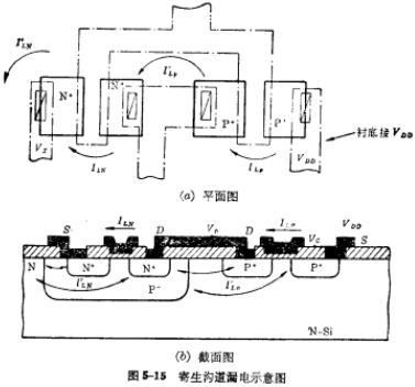
CMOS is a micro-power circuit, which has very strict requirements on power consumption. The main factor causing high power consumption is static leakage current. Therefore, in the process and layout design, special attention should be paid to taking appropriate measures to minimize leakage as much as possible. CMOS layout design summary. Figure 5-15 shows the main ways to generate leakage. Where  represents the oxide layer outside the channel of the load tube and the input tube Leakage below;
  and
and  means P+ source (or P+ leakage) and P- well, N+ Source (or N+ leakage) and N-Leakage of parasitic MOS tube between substrates.

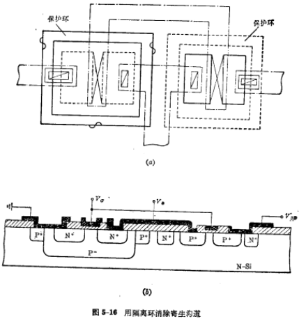
To eliminate parasitic leakage, an isolation ring must be used in layout design to interrupt the parasitic channel. Figure 5-16 shows that the active device is surrounded by a diffusion ring of the same type as the substrate. Diffuse the P+ isolation ring in the P- well region to cut off the parasitic N-type channel, and diffuse N- on the N- substrate sup>+ isolation ring to cut off the P-type parasitic channel.

As you can see from the picture, there are two N+ and P+ isolation ring The area of the parasitic leakage channel will not occur. So these areas are safe areas for interconnecting lines. CMOS layout design summary. Because to cause a parasitic inversion layer on the high-concentration diffusion ring, a very high voltage is required, and the power supply voltage of the actual circuit is much lower than the field-induced turn-on voltage, thereby eliminating the path of parasitic leakage.
2, drawing size regulations
(1) Graphic mark
CMOS usually has six mask patterns: ①P well diffusion area pattern; ②P channel MOS tube Original leak and P+Isolation ring diffusion zone Graphics; ③N-channel MOS transistor source and drain and N+ isolation ring diffusion area graphics; ④Gate and lead pattern; ⑤Contact hole (lead Hole) graphics; ⑥ metal electrode graphics.
According to the regulations of the original CMOS circuit joint design meeting of the Ministry of Four Machinery, the symbols used in the current CMOS circuit diagram are shown in Figure 5-17.

(2) Minimum layout size
The minimum size in layout design is related to the level of craftsmanship. The following layout dimensions do not represent the current technological level and are only for readers' reference.
Small-scale circuit (unit: μm)
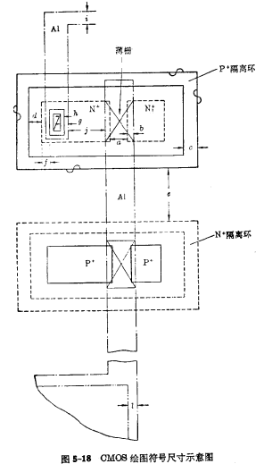
(a)channel length 10; (b )Grate coverage (each side) 5; (c) Diffusion zone width 12.5; (d) Diffusion zone spacing 12.5; (e)The distance between P well and N isolation ring is 20; (f)< /strong>The distance between the lead hole and the edge of the diffusion zone is 7.5; (g)Aluminum covered lead hole5, lead hole 10×12.5; (h) each side of the pre-engraved lead hole is 2.5 larger than the hole; (i) the width of the aluminum bar is 12.5; (j) Aluminum strip pitch 12.5, bonding point 120×120, bonding point pitch 120; (k) distance between bonding point and die edge 100; (l) passivation version is better than aluminum The bonding point is smaller by 7.5 on each side, and the chip separation line to the die pitch is 300.
Small-scale circuits can generally be drawn at a scale of 500 times. CMOS layout design summary. Medium-scale circuits can be drawn with 800 times the scale or 400 times the scale of the original picture. The minimum size of the medium-scale circuit is slightly smaller than that of the small-scale circuit, such as: the length of the channel is 8~10; the width of the diffusion zone is 8~10; the lead hole is 5 from the edge of the diffusion zone , Aluminum covers the lead hole 2.5~3, and the lead hole is 8×12.
The basic sizes and drawing symbols listed above are indicated in Figure 5-18.
3. Examples of tall graphics
According to the calculated device size, graphic mark and drawing size regulations, the configuration diagram of each device can be drawn.

(1) Two-input "NOR" gate configuration diagram
Figure 5-19 is the actual configuration of the two-input NOR gateExample. With such a configuration diagram, the device arrangement is relatively regular, the wiring is relatively neat, and the wafer area is fully utilized.
(2) CMOS transmission gate configuration diagram
Figure 5-20 is the configuration diagram of the CMOS transmission gate. In the picture, the N tube of the CMOS transmission gate and the N tube of the CMOS inverter are placed in a P -In the well, you can save the chip area of .
4. Gate protection device
The CMOS circuit is the same as the single channel circuit, and the input must also be protected.circuit, so it must be considered in the graphic design. There are generally two types of protection circuits commonly used in CMOS circuits.
(1) Single diode protection circuit
This type of protection the diode connection method of the circuit has two forms, one is to connect the diode between the input terminal and the ground. As shown in Figure 5-21; the other is to connect a diode between the input terminal and the power supply , As shown in Figure 5-22.
(2)电阻二极管保护电路
图5-23为电阻二极管保护电路的形式,在图中,D1为N+型扩散在P阱上形成的二极管,击穿电压 为P+型扩散在衬底上形成的二极管,击穿电压
 为保护电阻,是P型扩散在N型村底上形成的扩散电阻,这个电阻本身也形成二极管D2,所以不必单独制作,R的数值在500~1000Ω之间。
The steps and other principles of CMOS circuit general drawing are similar to single-channel MOS circuits, so I won’t go into details here.
Contact: Mr. Zou
Tel: 0755-83888366-8022
Mobile: 18123972950
QQ: 2880195519
Address: 5C1, CD Block, Tianji Building, Tian’an Digital City, Chegongmiao, Futian District, Shenzhen
Please search WeChat Official Account: "KIA Semiconductor" or scan the following picture to "Follow" Official WeChat Official Account
Please "Follow" the official WeChat account: provide MOS tube technical assistance


