Electronic Technology Forum
The main advantages of silicon gate process and detailed explanation of its application
"Silicon gate process" is a process that uses doped polysilicon to make the gate electrode of the MOS tube. The difference from the conventional aluminum gate process described above is that the silicon A thin layer of silicon dioxide (gate dielectric) is grown on the chip, and then a thin layer of polysilicon of about 500nm is deposited, and then the source and drain diffusion regions are carved out for source and drain diffusion. "Silicon gate process" has more characteristics for the performance of devices and integrated circuits than the conventional aluminum gate process.
First, the main advantages of silicon gate technology
1. Appropriate threshold voltage VT
In the PMOS structure of the aluminum gate, the contact potential difference between the metal and the semiconductor silicon varies with the semiconductor doping concentration.
For the silicon gate MOS structure, two situations can be considered:
(1) P-channel silicon gate situation
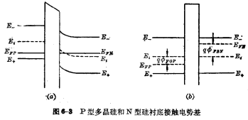
Namely P-type polysilicon and N-type silicon substrate, the contact potential difference is:
 ,As shown in Figure 6-3.

like ,It can be found from Figure 1-15:
 。
。
It can be seen from the threshold voltage formula that the difference between the threshold voltage of the aluminum gate and the silicon gate device is the difference between the contact potentials of the two, namely:

If P-type polysilicon is heavily doped, it means  , the threshold voltage of silicon gate P-channel MOS transistor is lower than that of aluminum gate VT is 1.1V lower in value.
(2) N-channel silicon gate process
i.e. N-type polysilicon and P-type substrate, the contact potential difference is:  If
If ,
,  , you can find:
 < /span>
If the NMOS structure composed of aluminum gate, when  , you can get
  . Therefore, the threshold voltage difference between the aluminum gate and the silicon gate device is:

This shows that the threshold voltage of the silicon gate process can be higher than that of the aluminum gate process N-channel MOS transistor.
From the above analysis, we know that silicon gate PMOS devices have a lower threshold voltage, which can reduce the working voltage of the circuit, so that it can be compatible with bipolar circuits. For CMOS circuits, the threshold voltage of NMOS devices and PMOS devices can be better matched.
2, with self-alignment function
Since polysilicon can withstand a higher diffusion temperature, you can make the gate oxide layer and polysilicon electrode first, and then perform source-drain diffusion. In this way, it has a self-alignment effect, which greatly reduces the overlapping parasitic capacitance of the gate source and the gate drain, thereby improving the performance of the circuit.
3. Realize multilayer wiring
The sheet resistance of doped polysilicon can be made relatively low, less than 100Ω/□. Therefore, the polysilicon strip can be used as an additional interconnection lead in the circuit. Because the passivation layer is formed on the surface of the polysilicon, the aluminum lead strip can be freely passed on it to implement multi-layer wiring.
4. Small chance of contamination by impurity ions
In the silicon gate process, after the gate oxide film is formed, the polysilicon electrode is deposited immediately, so during the entire process, the chance of the oxide layer being contaminated by impurity ions will be greatly reduced , The stability of the device is improved.
5. Small device size
Since the silicon gate process has self-alignment, the silicon gate MOS circuit can be made smaller than the aluminum gate MOS with similar performance, which is beneficial to improve integration Spend.
Silicon gate by hand has the above advantages and has been widely used in the field of MOS technology. Usually silicon gate technology is used to make P-channel and N-channel MOS circuits and CMOS circuits. And E/DMOS circuit.
Contact: Mr. Zou
Tel: 0755-83888366-8022
Mobile: 18123972950
QQ: 2880195519
Address: 5C1, CD Block, Tianji Building, Tian’an Digital City, Chegongmiao, Futian District, Shenzhen
Please search the WeChat official account: "KIA Semiconductor" or scan the picture below to "Follow" the official WeChat official account
Please "Follow" the official WeChat account: provide MOS tube technical assistance


