Electronic Technology Forum
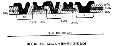
SiO2-AI2O3 double gate E/DMOS circuit overview
BecauseAI2O3layer It contains negative charge, which can offset the positive charge in SiO2, so it can control SiO2 and AI2O3Thickness ratio, so that the threshold voltage of NMOS becomes a positive value. Figure 6-28 uses SiO2-AI2O3. Technology-manufactured N-channel E/DMOS circuit. The substrate is 10Ω·cm,<100>P-type silicon single chip. For the depletion type device, after the gate is oxidized, a phosphorous treatment is performed, and the threshold voltage is controlled to be 1.5V. For enhanced devices, after gate oxidation, a layer is depositedAI2O3, threshold The voltage is controlled at +1V. This circuit can work under a 5V power supply.

Contact: Mr. Zou
Tel: 0755-83888366-8022
Mobile: 18123972950
QQ: 2880195519
Address: 5C1, CD Block, Tianji Building, Tian’an Digital City, Chegongmiao, Futian District, Shenzhen
Please search the WeChat official account: "KIA Semiconductor" or scan the picture below to "Follow" the official WeChat official account
Please "Follow" the official WeChat account: provide MOS tube technical assistance


