Electronic Technology Forum
Detailed explanation of MOS field effect tube characteristic curve and three working areas
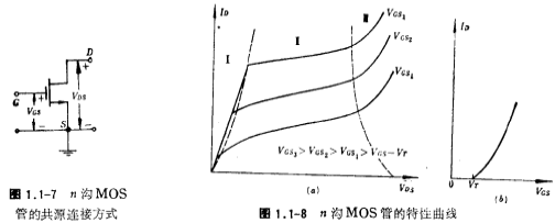
Take the n-channel enhanced MOS transistor as an example for discussion. MOS field effect tube has a variety of connection methods in applications, the most commonly used is common source connection, as shown in Figure 1.1-7. In the figure, the source is connected to the substrate, and the signal is input by the gate G, and output by the drain D after being amplified by the MOS field effect tube. When the GS voltage VGS changes, the output characteristic curve of the n-channel enhancement mode MOS FET is shown in Figure 1.1-8b. The transfer characteristic curve is shown in Figure 1.1-8b, which reflects the relationship between the drain-source current ID and the gate bias voltage VGS. VT in the picture is called the threshold voltage, it characterizes the critical operating point of the MOS field effect tube transition from cut-off to conduction. Only when the gate bias voltage is higher than VT, the MOS field effect transistor can be turned on.

The output characteristic curve in 1.1-8a can be divided into three working areas by the dotted line in the figure, namely, the resistance zone (I), the saturation zone (Ⅱ) and the lightning The collapse area (Ⅲ), the main characteristics of each area are briefly explained below. It is assumed here that the source is connected to the substrate.
1. Adjustable resistance area (also called linear area)
In this area, ID follows VDs is similar to the linear change, so it is also called the linear region. According to the basic knowledge of semiconductor surface, if the doping concentration of p-type substrate is constant, when VGS>VT, an n-type inversion layer will appear on the surface of the gate oxide layer, that is, a field-induced conductive channel between the source region and the drain region, as shown in Figure 1.1-9a However, if the drain-source voltage is zero at this time, the potentials in the channel are the same everywhere, so the drain-source current cannot be formed, that is, ID is zero. Characteristic curve of MOS field effect tube. When VDS>0, there will be horizontal Potential gradient, so a current is formed between the drain and the source. And when VDS increases, the lateral potential gradient increases, and the current ID also increases, ID and VDS changes linearly. At this time, the channel induced between the source region and the drain region is equivalent to a linear resistance. Corresponding to different VGS, the channel resistance value will also change. For example, when VGS increases, the channel thickness increases, so the channel The resistance will decrease.
In addition, when VDS>0, due to the lateral potential gradient in the channel, the vertical electric field intensity near the source in the channel region is greater, and the vertical electric field near the drain The electric field strength is small, which causes the channel thickness from the source to the drain to gradually become thinner, which will increase the channel resistance significantly. Therefore, at this time, the ID increases with VGS at a slower rate, and an adjustable resistance zone appears. In the curved part.
WhenVDS Continue to increase to VDS-VT, the voltage between the gate and drain is exactly equal to the turn-on voltageVT, so the inversion layer on the silicon surface near the drain end disappears, leaving only the depletion region, that is, the channel thickness is zero here (the channel at the drain starts to pinch off), As shown in Figure 1.1-9b. This situation corresponds to the junction of the adjustable resistance zone and the saturation zone in the output characteristic curve. After that, the drain current begins to saturate.
2, saturation area
In the saturation region, ID hardly changes with VDS, so it is called the drain current saturation region. When VDS>VT-VT, the voltage between the drain and the gate is less than VT, and the area where the channel thickness is zero is slightly enlarged, that is, the pinch-off point is closer to the source, as shown in the figure shown in 1.1-9c. Characteristic curve of MOS field effect tube. At this time, when VT increases, the increased voltage is basically applied to the depletion region where the channel thickness is zero. Since the voltage across the channel is basically unchanged, when VDS increases, the drain current does not increase and reaches the saturation value. Of course, if VGS increases, the saturation current value is also due to the decrease in channel resistance. Correspondingly, the saturation area is the main working area of the MOS field effect tube.

3、Avalanche zone
If VDS is greater than a certain breakdown voltage BVDS, reverse breakdown of the Pn junction between the drain and the substrate will occur, ID will increase sharply, and the characteristic curve will enter the avalanche zone (Ⅲ). At this time, the drain current does not pass through the channel region, but directly flows into the substrate from the drain. When designing the circuit, avoid the MOS field effect tube working in the avalanche zone.
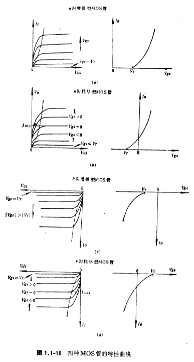
Usually the output characteristic curve of n-channel enhancement mode MOS FET can be divided into four districts (see Figure 1.1-10a).
(1)Deadline: 。
。
(2)Linear zone (adjustable resistance zone): ,
, ,ID and VDS are approximately linear. At this time, the drain and source ends of the MOS tube are equivalent to a linear resistor, and its resistance is affected by
 control,
 the larger the value, the smaller the resistance value.
(3)Saturation zone: ,
, at this time, with the increase of VDS, the ID change is small, and the size of the ID is mainly determined by
 to determine the voltage value,
 the larger the ID, the larger the ID.
(4)Avalanche area: at this time, ID increases rapidly with the increase of VDS.
The main difference between the n-channel depletion mode MOS field effect transistor and the n-channel enhancement mode MOS field effect transistor is that the p-type substrate of the former has a lower doping concentration, so when When it is zero, the silicon surface under the gate has formed an inversion layer, that is, a channel has been formed. Therefore, a considerable drain current can be formed by adding a certain drain-source voltage, and only a larger drain current can be formed on the gate. Negative voltage can change the surface under the gate from inversion to depletion. At this time, the n-channel disappears and the drain current becomes zero. The gate-source voltage when the drain current is zero is called the pinch-off voltage of the n-channel depletion MOS field effect transistor (using
 or
or represented), the characteristic curve of n-channel depletion MOS field effect transistor is shown in Figure 1.1-10b, and its shape is completely similar to that of the enhanced type. Depletion FET
 the saturation current at the time is denoted as IDSS, which is often referred to as the drain-source saturation current.
For the sake of comparison, Figure 1.1-10c and d respectively show the characteristic curves of p-channel enhancement mode and depletion mode MOS field effect transistors. The output characteristic curve of P-channel MOS field effect transistors is similar to that of n-channel. Only in normal operation, the voltage polarity and the direction of the drain current of the P-channel device are opposite to those of the n-channel device.
The above qualitative discussion of the working principle of MOS field effect tube, the following will quantitatively calculate the threshold voltage of MOS field effect tube, and list the relationship between VT and ID and VDS, VGS.

Relevant information
Basic principles and characteristics of MOS field effect transistors
Basic structure and working principle of MOS field effect tube
The type of MOS field effect transistor
Contact: Mr. Zou
Tel: 0755-83888366-8022
Mobile: 18123972950
QQ: 2880195519
Contact address: 5C1, CD Block, Tianji Building, Tian’an Digital City, Chegongmiao, Futian District, Shenzhen
Please search the WeChat official account: "KIA Semiconductor" or scan the picture below to "Follow" the official WeChat official account
Please "follow" the official WeChat account: provide MOS tube technical assistance


