Electronic Technology Forum
Detailed explanation and characteristics of the basic principles of MOS field effect transistors
Generally, quality control can be divided into two major categories, one is called "bipolar" transistors, this type of transistor works, electrons and holes participate in conduction; The other type is called a "field effect" transistor, which is a semiconductor device that uses a change in the electric field perpendicular to the conduction channel to control the conduction ability of the conduction channel, thereby achieving amplification. The basic principle of MOS field effect tube. This kind of transistor has only one type of carrier-electron or hole-which plays the main role of transporting current. Therefore, the "field effect" transistor is also called "unipolar" transistor, which means that there is only one type. Carriers of polarity participate in conduction to distinguish it from "bipolar" transistors.
Field effect transistors can be divided into three types: insulated gate field effect transistors (IGFET), junction field effect transistors (JFET) and thin film field effect transistors.
The insulated gate field effect transistor consists of a gate, an insulating layer (usually an oxide layer) and a semiconductor. The most common IGFET has its gate made of metal and the insulating layer is made of oxide Layer (SiO2), and the conductive channel is made of semiconductor silicon material, so it is also called MOS field effect tube, which is the mainstream of FET at present. In recent years, it has developed rapidly, and this book is limited to discussing the principles of MOSFETs.
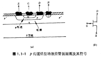
Junction FET is a kind of FET constructed by using the field effect in the semiconductor body. Figure 1.1-la is a cross-sectional view of a p-channel (referred to as P-channel) junction field effect transistor (JFET). Its electrodes include gate G, source S, drain D, and substrate (or bottom gate) B. The basic principle of MOS field effect tube. In use, the top gate G is often connected to the substrate B. At this time, the JFET becomes a three-terminal device, and its symbol is shown in Figure 1.1-1b.

From the structural point of view, the p-channel junction field effect transistor is characterized by being fully compatible with the bipolar process, and the p-type diffusion regions of the source and drain are compatible with the bipolar process. The base area diffusion of the bipolar nPn tube is completed at the same time. In principle, the top gate of the n+ area can be the same as the emitter's n+The diffusion area is formed at the same time, so it can be used in bipolar analog integrated circuits without adding process steps. The working principle of junction field effect transistors is different from that of MOS field effect transistors. The basic principle of MOS field effect tube. It changes the barrier originality of the pn junction between the gate and source by changing the gate-source voltage, thereby controlling the conductivity of the channel region and realizing the amplification function. Because its basic structure is still a Pn junction, it is called a junction field effect tube to distinguish it from a MOS field effect tube.
Under the current process conditions, junction FETs have better stability and lower noise than MOS FETs. However, due to its shed-source It is a reverse biased pn junction, its input resistance will be lower than the MOS field effect tube, of course it is still much higher than the nPn tube.
The working principle of junction FET is different from that of MOS FET, but the relationship between current and voltage is basically the same.The same, so the analysis method of MOS FET circuit is also suitable for junction FET circuit.
related information
(1) Basic structure and working principle of MOS field effect tube
(2) Types of MOS field effect transistors
(3) Characteristic curve of MOS field effect tube
Contact: Mr. Zou
Tel: 0755-83888366-8022
Mobile: 18123972950
QQ: 2880195519
Contact address: 5C1, CD Block, Tianji Building, Tian’an Digital City, Chegongmiao, Futian District, Shenzhen
Please search the WeChat official account: "KIA Semiconductor" or scan the picture below to "Follow" the official WeChat official account
Please "follow" the official WeChat account: provide MOS tube technical assistance


