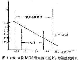
MOS transistor threshold voltage temperature effect, in order to make the MOS field effect transistor work stably and reliably within a certain temperature range, the design must consider adapting its
MOS transistor threshold voltage temperature effect, in order to make the MOS field effect transistor work stably and reliably within a certain temperature range, the design must consider adapting its
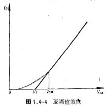
MOS tube should have sub-threshold effect, which is also called weak inversion effect. So far, we have assumed that when the voltage applied to the gate of the MOS tube exceeds the threshold voltage,
MOS tube should have sub-threshold effect, which is also called weak inversion effect. So far, we have assumed that when the voltage applied to the gate of the MOS tube exceeds the threshold voltage,
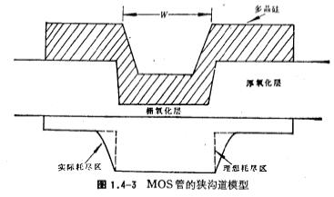
The narrow channel effect of MOS tube, the first-level approximate simulation of MOS field effect tube is given above, and some important relations are deduced under similar conditions. These are undo
The narrow channel effect of MOS tube, the first-level approximate simulation of MOS field effect tube is given above, and some important relations are deduced under similar conditions. These are undo
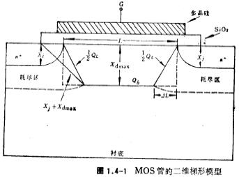
Short-channel effect of MOS tube The first-level approximate simulation of MOS field effect tube is given above, and some important relations are deduced under similar conditions. These are undoubted
Short-channel effect of MOS tube The first-level approximate simulation of MOS field effect tube is given above, and some important relations are deduced under similar conditions. These are undoubted
The AC small-signal model of MOSFET, the large-signal model of MOS field effect tube was discussed above, we can deduce the AC small-signal model of MOS field effect tube from the large-signal model o
The AC small-signal model of MOSFET, the large-signal model of MOS field effect tube was discussed above, we can deduce the AC small-signal model of MOS field effect tube from the large-signal model o
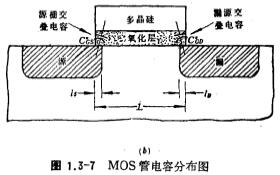
MOS capacitor model, the five capacitors in the MOS tube large signal model (see Figure 1.3-1b), the image.png and image.png are image.png junction barrier capacitors, image.png, image.png and image.p
MOS capacitor model, the five capacitors in the MOS tube large signal model (see Figure 1.3-1b), the image.png and image.png are image.png junction barrier capacitors, image.png, image.png and image.p
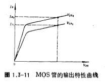
The DC characteristics of MOS field effect transistors, n-channel enhancement mode MOS, for example, discuss the current-voltage characteristics of the MOS transistor before the channel is pinched off
The DC characteristics of MOS field effect transistors, n-channel enhancement mode MOS, for example, discuss the current-voltage characteristics of the MOS transistor before the channel is pinched off

MOS field effect tube model. In the analysis and design of MOS large-scale integrated circuits, computer-aided circuit simulation has become the basic method of circuit design. The MOS field effect tu
MOS field effect tube model. In the analysis and design of MOS large-scale integrated circuits, computer-aided circuit simulation has become the basic method of circuit design. The MOS field effect tu
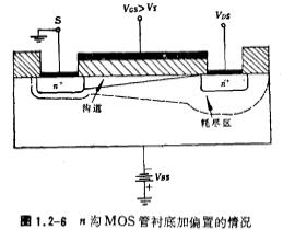
In a MOS integrated circuit composed of many MOS tubes, many tubes are built on the same substrate. At this time, it is impossible to connect the sources of all MOS tubes to a common substrate, and th
In a MOS integrated circuit composed of many MOS tubes, many tubes are built on the same substrate. At this time, it is impossible to connect the sources of all MOS tubes to a common substrate, and th

The difference between an actual MOS tube and an ideal MOS tube is that the threshold voltage (unit area) of the positively charged N-channel MOS field effect tube in the oxide layer and the contact p
The difference between an actual MOS tube and an ideal MOS tube is that the threshold voltage (unit area) of the positively charged N-channel MOS field effect tube in the oxide layer and the contact p


5C1, CD Block, Tianji Building, Tianan Digital City, Futian District, Shenzhen

KIA-The Public