Electronic Technology Forum
Analysis of the characteristics of MOS field effect transistor threshold voltage
For enhanced tubes, the threshold voltage is the turn-on voltage VTFor a depletion tube, the threshold voltage is the pinch-off voltage VT, For convenience, it is also represented by VT. The threshold voltage VT is defined as, when VDS=0, The gate voltage required to form a strong inversion conductive channel on the semiconductor surface between the source and the drain is called the threshold voltage.
Threshold voltage is an important parameter of MOS devices, and it is closely related to device process parameters.
When calculating the threshold voltageVT Before, let's first discuss the physical properties of the silicon surface.
First, the physical characteristics of the silicon surface of the MOS tube
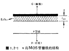
The structure of the gate part of the n-channel MOS tube is shown in Figure 1.2-1.
Grow a layer of SiO2 oxide layer on p-type silicon, the thickness of which is  , usually
  is 600~1000 Angstroms. The material covered on the SiO2 oxide layer is aluminum or polysilicon, which forms the gate. B is the lead-out pin of the substrate. Threshold voltage of MOS field effect tube. If the substrate B is grounded, and a different voltage VG is applied to the gate G, then the surface of the silicon (silicon and SiO2 The charge distribution is different. According to the charge distribution on the silicon surface, it can be divided into accumulation, depletion and inversion. Discuss separately as follows:

1、accumulation
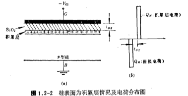
When a negative voltage (-VG) is applied to the gate G, the number of holes near the silicon surface increases due to the electrostatic induction of the gate oxide capacitance, and the surface layer changes from P-type to strong P-type, that is, holes are formed on the surface Accumulation layer. Figure 1.2-2a.b shows the charge distribution when the accumulation layer and the accumulation layer are formed on the surface, respectively.

2、Run out
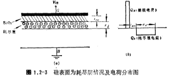
When a positive voltage is applied to the gate G at this time, due to the electrostatic induction of the gate oxide capacitance, the movable hole charge is repelled downwards, leaving a static negative charge region of acceptor impurity ions near the surface, forming a depletion layer, the thickness of the depletion layer Denoted as
 figure 1.2-3a and b respectively show the charge distribution of the depletion layer and the surface of the depletion layer.
According to the principle of conservation of charge, the charge on the gate and the charge in the depletion layer
 should be equal, i.e.
 , or written as
 . Now calculate the thickness of the depletion layer
 。
。

Suppose the doping concentration of the p-type substrate is , It turns out that an infinitely small thin layer on the P-type substrate
 the movable hole charge dQ is:

In order to transfer this part of the charge, the potential change dф on the surface of the substrate is:

here, is the relative permittivity of silicon material, its value is 11.8;
 is the vacuum permittivity, its value is 8.85×10⁻¹⁴ method/cm;
 it can be understood as the capacitance of the depletion layer per unit area; q is the amount of electronic charge. Integrate both sides of the above formula to get:

in
 represents the Fermi potential of the substrate in the equilibrium state,
 is the intrinsic carrier concentration (at room temperature
 ),
), is Boltzmann's constant and T is the absolute temperature.
when when, the thickness of the depletion layer can be obtained

After the movable hole charge is repelled out of the depletion layer, a static acceptor ion charge per unit area is left Can be expressed as

3、Inversion
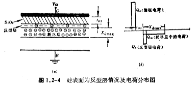
When a positive voltage is applied to the grid G is further enlarged, and a movable negative charge is generated on the surface of the silicon, and the surface is changed from p-type to n-type, that is, the surface is inverted. An inversion layer is formed on the surface, and the inversion layer is the channel in the MOS tube. Threshold voltage of MOS field effect tube. According to the semiconductor energy band theory, when the surface potential changes
  , The surface is inverted, and the negative charge density in the channel of the inversion layer is the same as the hole charge density in the original equilibrium state. This phenomenon is defined as strong inversion. As VG further increases, the value of the surface potential and the thickness of the depletion layer
 There will be no more obvious changes, so in the case of strong inversion, the thickness of the depleted layer reaches the maximum value, which is recorded as
  , its expression can be written as

The static charge of the depletion layer per unit area is

Figure 1.2-4 shows the charge distribution when the surface is inverted. According to the principle of conservation of charge and Figure 1.2-4b, 。
。

Related information
the threshold voltage of ideal MOS field effect transistor (VDS=0)
the threshold voltage of the actual N-channel MOS tube (VBS=0)
the influence of the substrate bias effect (body effect) on the threshold voltage a>
Contact: Mr. Zou
Tel: 0755-83888366-8022
Mobile: 18123972950
QQ: 2880195519
Contact address: CD, Tianji Building, Tian’an Digital City, Chegong Temple, Futian District, Shenzhen Block 5C
Please search WeChat official account: "KIA Semiconductor" or scan the following image" Follow "Official WeChat Official Account
Please "Follow" the official WeChat account: Provide MOS tube technical assistance


