Electronic Technology Forum
Analysis of the types and characteristics of MOS field effect transistors
The previous section took the n-channel enhancement mode MOS field effect transistor as an example, and qualitatively explained the working principle of the field effect tube. If distinguished by different conductive channels, there is another P-channel enhancement mode MOS field effect. Tube. The type of MOS field effect tube. This tube uses n-type semiconductor as the substrate material, and the source and drain regions are p+ diffusion regions. In Figure 1.1-3, replace n+ with p+, p-type silicon with n-type silicon, and n-channel with p-channel Road, that is, a cross-sectional view of the P-channel MOS field effect tube structure. It is also an enhanced tube, because when the gate voltage is zero, there is no conductive channel between the source and drain regions. In normal operation, the source is generally grounded, and the drain area is connected to a negative potential. When a negative potential is applied to the gate, there is a surface electric field pointing to the outside on the surface of the n-type semiconductor, which depletes the surface and can even be inverted. (at this time
 ) When the n-type surface is strongly inverted into p-type, the p+ regions of the source and drain are connected. At this time, if a negative voltage is applied to the drain, current will flow. It can be seen from the above analysis that the working principles of n-channel and p-channel devices are basically the same, except that the polarities are opposite and the conductive channels are different. When the n-channel enhanced tube is working, the gate and drain are both connected to a positive voltage, which is similar to the nPn tube in the bipolar type. The type of MOS field effect tube. The current-carrying carriers are holes, and the threshold voltage VT is positive.
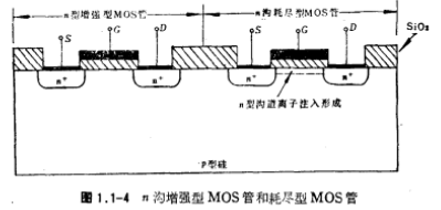
In addition to enhanced field effect transistors, there is also a type called depletion transistors, the common ones are n-channel depletion transistors, as shown in Figure 1.1-4. Its main feature is that when no voltage is applied to the gate, the n-type channel already exists. This can be achieved by controlling a certain amount of positive charge in the oxide layer or by ion implantation. When a negative voltage VGS is applied to the gate of the n-channel depletion transistor, the conduction of the channel will decrease, and under the action of a certain VDS, the IDS flowing through the channel will decrease. If the absolute value of VGS increases, IDS continues to decrease. when at this time, it will completely offset the influence of the positive charge in the oxide layer on the p-type surface, and make the original n-type sensing channel completely disappear. At this time, even if a positive voltage VDS is applied to the drain, no current will flow. . We say that the tube is cut off at this time. The gate voltage (threshold voltage) required to turn off the depletion tube (the surface channel disappears) is called the cut-off voltage (VT). Obviously, the n-channel depletion tube has VT<0.

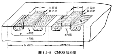
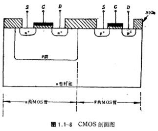
In Figure 1.1-4, the P substrate simultaneously forms an n-channel enhancement type field effect transistor and an n-channel depletion type field effect transistor. This structure and process are usually called E/DMOS, which is a type of NMOS. The type of MOS field effect tube. In addition, on the same substrate, P-channel MOS field effect transistors and n-channel MOS field effect transistors are generated. This structure and process are usually called CMOS. Due to the simple structure of CMOS circuits and low power consumption, in MOS integrated circuits, CMOS circuit structure and technology are widely used. The structure diagram and cross-sectional diagram of CMOS circuit are shown in Figure 1.1-5 and Figure 1.1-6 respectively.


In principle, there is also a P-channel depletion type device, which is different from the n-channel depletion type in that n-type silicon is used as the substrate. This kind of tube requires that when no voltage is applied to the gate, there is a P-type channel on the surface between the source and the drain. If the source is connected to the substrate and grounded, as long as a negative voltage is applied to the drain terminal, the holes can be Flow between the drain and the drain to form a drain-source current; when a positive voltage is applied to the gate, the concentration of holes in the channel decreases, the conductivity is weakened, and the drain-source current decreases. The voltage applied to the gate to make the surface channel disappear is VT. Obviously, for the P-channel depletion transistor . The type of MOS field effect tube. Because the p-channel depletion MOS is difficult to manufacture and its characteristics are not as good as the n-channel MOS, there are few practical applications.
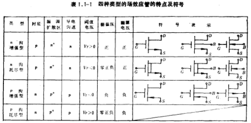
In summary, there are four types of field effect transistors, which are n-channel enhancement type, n-channel depletion type, P-channel enhancement type, and P-channel depletion type. Table 1.1-1 lists the characteristics of the above four types of MOS field effect transistors and three commonly used symbols.

Related information
The basic principles and characteristics of MOS field effect transistors
Basic structure and working principle of MOS field effect tube
Characteristic curve of MOS field effect tube
Contact: Mr. Zou
Tel: 0755-83888366-8022
Mobile: 18123972950
QQ: 2880195519
Contact address: Che Gong, Futian District, Shenzhen 5C1, CD Block, Tianji Building, Tianan Digital City, Temple
Please search WeChat public account: "KIA Semiconductor "Or scan the picture below to "Follow" the official WeChat account
Please "Follow" the official WeChat account: Provide MOS tube technical assistance


