Electronic Technology Forum
Analysis of the basic process steps of the main process of VMOS
(1) Once oxidation
On the N- epitaxial layer with (100) plane N+-Si as the substrate, grow a Layer silicon dioxide mask. As shown in Figure 6-26(a).
(2) Lithography, boron diffusion
The boron diffuses to form the P area of the substrate, and the diffusion depth is about 2μm. As shown in Figure 6-26(b)
(3) Lithography, phosphor diffusion
Phosphorus diffuses to form a source region, the junction depth is about 1μm, and is deposited at low temperature to form a silicon dioxide protective film. As shown in Figure 6-26(c).
(4) Lithography, etching V-groove
Photoetch the V-groove window and etch the V-groove with hydrazine. As shown in Figure 6-26(d).
(5) Pre-engraved lead hole
The lead holes are pre-engraved, and the gate is oxidized, and the surface is treated with phosphorous. As shown in Figure 6-26(e).
(6) Electrode lead
Engrave lead holes, evaporate aluminum, and reverse engrave electrodes to complete electrode leads. As shown in Figure 6-26(f). So far, the chip is formed.

The above processes, except for the V-groove etching process, are all conventional planar processes. The corrosion of the V-groove is the most critical part. Because the channel of the VMOS transistor is next to the wall of the V-shaped groove, the quality of the corrosion has a significant impact on the characteristics of the VMOS.
V-shaped groove corrosion is based on the anisotropic chemical properties of Si single crystal. The main process of VMOS. The corrosive liquid can be hydrazine hydrate (namely hydrazine hydrate N2H4H< span style="font-size: 10px;">2O) or a mixture of water and isopropanol buffered KOH.
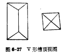
The corrosion process of the V-shaped groove is as follows: First, make the V-shaped groove hole on the (100) surface, and then put the film into the corrosion which is heated to 80~100℃ In the liquid, due to the rapid corrosion rate of the (100) surface, the exposed (100) surface quickly corrodes pits. The (111) crystal plane, which forms an angle of 54.74° with the (100) crystal plane, extends into the body along the four sides of the corrosion window to form a four-sided pyramid. As shown in Figure 6-27. Because the corrosion rate of the (111) crystal plane is extremely slow, when the surface of the etching window (100) is completely etched, the sidewalls of the etch pit are all limited by the (111) crystal plane, and the corrosion basically stops automatically.

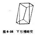
It must be noted that the edge of the lithography window must be strictly parallel or perpendicular to the<110>direction. Distortion occurs, as shown in Figure 6-28. The main process of VMOS. Therefore, when designing the V-groove on the layout, special attention must be paid.

In addition to the aluminum gate VMOS, it can also be combined with silicon gate and other processes to make VMOS transistors and integrated circuits to further improve the performance of the device.
Although the VMOS process is complicated, it can be well controlled by careful operation. The main process of VMOS. Once the anisotropic corrosion technology becomes a very easy-to-operate conventional process, the VMOS process will be widely used to manufacture large-scale MOS integrated circuits.
Contact: Mr. Zou
Tel: 0755-83888366-8022
Mobile: 18123972950
QQ: 2880195519
Address: 5C1, CD Block, Tianji Building, Tian’an Digital City, Chegongmiao, Futian District, Shenzhen
Please search the WeChat official account: "KIA Semiconductor" or scan the picture below to "Follow" the official WeChat official account
Please "Follow" the official WeChat account: provide MOS tube technical assistance


