Electronic Technology Forum
Examples of MOS transistors in integrated circuits and analysis of wiring methods
This section gives an example of a MOS integrated circuit, describing how MOS transistors are constructed and connected in an integrated circuit.
(1) The concept of MOS transistor
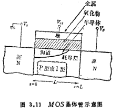
For ease of understanding, Figure 3.11 draws the cross-sectional structure of the MOS transistor. Applying a voltage to the capacitor of the MOS structure can induce charge on the surface of the semiconductor. The MOS transistor uses the conductivity of the induced charge to achieve its work. In the case of N-channel, if a positive voltage is applied to the gate, electrons will be induced in the semiconductor, increasing the current between the source and drain of the N region. An example of the structure of MOS in an integrated circuit. Therefore, the integrated circuit structure consists of two N-type regions in a P-type substrate. The insulating film covering between the two regions, the metal gate electrode, and the wiring between these electrodes are formed.

(2) Examples of integrated circuit structure
Figure 3.12 shows a partial enlarged photo of the N-channel MOS memory large-scale integrated circuit and the corresponding layout pattern. This part roughly includes half of the memory flip-flop circuit. The bottom half is the amplifier transistor, above it is the bit transistor for writing and reading, and the upper right corner is the power supply VDD. On the left is the load transistor.
Now we will use the bit transistor located in the center to illustrate the method of constructing the transistor.
The N-type diffusion zone is represented by a single diagonal line and is arranged on the upper and lower sides. The diffusion area on the upper side is dedicated to the bit transistor; the diffusion area on the lower side is shared with the drain area of the amplifying transistor. Extend to the left and then upwards, shared with the source of the load transistor.
In order to lead out the electrode from the upper N-type region, the oxide film in the cross-hatched portion in the N-type region should be removed, and the aluminum electrode should be covered here to form an ohmic contact.
In addition, the gate electrode and the lead are shared. The aluminum electrode partially overlapping the gap between the upper and lower diffusion regions traverses the left and right, and at the same time constitutes the gate region.
The load transistor in the upper part of Figure 3.12 is different from the above-mentioned bit transistor. The gate and drain of the load transistor are electrically connected together, and both are connected to the power supply voltage, which is a form of leaking grounded load. Examples of MOS structures in integrated circuits. Here, the gate electrode is in communication with the power supply VDD, and the entire aluminum electrode is covered. At the same time, in order to increase the resistance value of the load transistor and reduce its current, the gate width should be much smaller than the gate length, and it should be made into a slender shape in the source and drain direction.
(3) Wiring method
It can also be understood from Figure 3.12 that the cross-wiring of MOS integrated circuits is easier than bipolar. The topological structure of a bipolar transistor is that the emitter is surrounded by the base, and the base is surrounded by the collector. Therefore, in order to draw the electrode from the emitter, if it is not drawn from above through the base and collector parts of the covering insulating layer, it cannot be drawn elsewhere.
However, the source and drain of the MOS transistor are made by the same diffusion process in different regions. Therefore, in the case of N-channel, N-type regions are scattered everywhere on the P-type substrate. For the N-channel, there is only a positive potential in the circuit, and these N-type regions in the P-type substrate are zero bias or reverse bias. Therefore, this diffusion region can be used as a lead.
Now take the example in Figure 3.12 for illustration. The N-type region shared by the bit transistor and the amplifying transistor can extend to the left and then upwards, and is connected to the source of the load transistor. At this time, the gate electrode of the bit transistor also extends to the left and crosses the diffusion region. Examples of MOS structures in integrated circuits. This kind of intersection is the intersection of the diffusion layer and the aluminum lead, and the two are separated by an oxide film. The easy realization of such cross wiring is a feature of MOS transistors. Therefore, very complex large-scale integrated circuits do not need to be realized by multi-layer wiring.
What is worth noting in the design of MOS integrated circuits is to try not to generate parasitic MOS devices. As we will talk about in Section 3.2.4, there is a way to avoid the generation of parasitic MOS transistors, which is to thin the insulating film only in the part of the MOS transistor, and thicken the insulating film at other wiring locations. In Figure 3.12, the part represented by the dashed line from the bit transistor to the amplifying transistor is the part of the thin oxide film.
Contact: Mr. Zou
Contact number: 0755-83888366-8022
Mobile phone: 18123972950
QQ: 2880195519
Contact Address: 5C1, Block CD, Tianji Building, Tianan Digital City, Chegongmiao, Futian District, Shenzhen
Please search WeChat official account: "KIA Semiconductor" or scan the following picture to "Follow" official WeChat official account
Please "follow" the official WeChat account: provide MOS tube technical assistance


